4.1 Performance Requirements
4.1.1 Readout noise versus readout rate
These are a function of the characteristics of the particular CCD and of the CCD controller electronics. For example, with the current Keck I CCD controller electronics (HIRES) reading a Tektronix 2048 x 2048 pixel CCD, we have obtained readout noise of 5.5 electrons at a readout rate of 33 kilopixels/second, or a per-pixel time of 33 µsec. Of that 33 µsec, 16 are spent on signal integration (8 µsec on baseline, 8 on charge), 8 µsec on analog to digital conversion, and the remaining 9 µsec include the actual serial transfer, DSP overheads, and transmission of the pixel data down the fiber. With our current CCDs, as the signal integration time is decreased, we see a corresponding increase in readout noise. However, some of the chips currently under development (e.g., the Lincoln CCDs described in Chapter 3) are reported to achieve significantly lower readout noise even with relatively short signal integration time, although this may have been achieved by trading off dynamic range.
For DEIMOS, we have a readout noise requirement of 5 electrons and a goal to do significantly better if possible. This requirement is based on the calculation that the sky noise in the dimmest part of the spectrum for a moderate exposure (e.g., 2,000 seconds) will be about 10 electrons (see Figure 1.1).
We also have a goal of a readout rate of 100 kilopixels/second (or a per-pixel time of 10 µsec), provided that we can achieve the required readout noise at that rate (10 µsec yields a 42 sec readout time for the whole mosaic if all amplifiers are read in parallel. This is three times faster than our minimum spec of 120 s.). In order to achieve that rate, we need to significantly decrease the 33 µsec/pixel time of the Keck I UCSD CCD system. Much of this decrease will be accomplished by decreasing the ADC convert time from 8 µsec to 1, and reducing the serial transfer, DSP overheads, and transmission time down to 1-2 µsec. Depending on the extent to which these various operations can be overlapped, this leaves only 7-8 µsec for signal integration (e.g., 4 on baseline, 4 on charge). It is hoped that the CCDs currently under development will be able to meet the readout noise requirement with signal integration times of this order or shorter.
4.1.2 Gain / Stability
We will have a high gain mode of about 1e-per DN. With a 16-bit ADC, that gives us an effective full well of 64K. Depending on the native full well of the chip, we may also implement a low-gain mode of about 2e- per DN. Within a factor of two, this means we will saturate on a star of 13.0 V mag in 1 sec in high-gain mode in good seeing.
The overall gain of the system should remain stable to 0.5% over a 2 C temperature change. This is a function of the temperature stability of the components on the external preamplifier board and on the analog boards of the CCD Controller electronics. As the Controller will be contained in a thermally-controlled enclosure, the temperature variations should be held within this range. The temperature stability of the preamp will have to be carefully checked.
4.1.3 Linearity of Electronics
The linearity of the system should be within 0.5% up to the full range of the 16-bit ADC, which is 64K DN.
4.1.4 A/D Converter Accuracy
The ADC will provide a resolution of 16-bits, with an accuracy of 1 bit. A histogram of a digitized signal should confirm that there are no missing or preferred ADC codes. Since these devices can degrade over time, the performance of the ADCs in the CCD Controller analog electronics should be checked not only during installation, but at periodic intervals thereafter as part of a preventive maintenance program.
4.1.5 Bias Frames
4.1.5.1 Flatness Specification
The signal level from bias frames should be flat across each row (including both the prescan and overscan regions) to within 1 ADC unit.
4.1.5.2 Limits on Correlated Noise
The Fourier spectrum of the signal obtained along any given (defect-free) row or column should be free of any significant peaks indicating periodic or correlated noise sources (e.g., 60 Hz noise from power lines, 20 KHz noise from switching supplies, etc.). The goal is that the Fourier amplitude of all components up to the Nyquist frequency should be less than 1e-. To meet this spec, the average of the overscan pixels in each row may be subtracted first.
4.1.6 Bias Match Among Individual CCDs and Amplifiers
Mechanisms must be provided to insure adequate matching of the bias levels between amplifiers on the same CCD, as well as between CCDs that are part of the same mosaic. The goal is to get the bias levels of all amplifiers in a mosaic equal to within 5 ADU. This match may be accomplished by both analog and digital adjustment. In the UCSD I CCD Controller, the bias level of each amplifier can be adjusted via a video offset level generated by a DAC which is coupled into the video processing chain. Unfortunately, the resolution of this DAC does not provide adequately fine adjustment, so that it is nearly impossible to obtain matched bias levels between the two amplifiers during multi-amplifier readouts. As a result, the two halves of an image obtained in this mode do not have consistent bias levels, and it becomes extremely difficult to set the color map to a range that provides appropriate contrast on both sides.
To overcome this limitation, we propose that an additional level of adjustment be provided digitally via software through the use of a separate numeric offset for each amplifier channel. During readout, the respective offset for each amplifier would be subtracted from the raw data in real-time as it is transmitted from the CCD controller.
4.1.7 Gain Match Among Individual CCDs and Amplifiers
A similar mechanism must be provided to insure adequate matching of the gains between amplifiers on the same CCD, as well as between CCDs that are part of the same mosaic. The goal is that all gains should match to within 1%. If possible, this match should be accomplished by analog adjustment, in order to avoid the need for floating point calculations in the CCD Controller. Provided that separate bias voltages are supplied to each amplifier (see Section 4.1.10 below), careful adjustment of the ratio of voltages to each quadrant should allow the gains to be equalized. The limiting factor is the resolution by which the bias voltages can be adjusted. In the existing UCSD I Controller, the adjustment is fairly coarse, about 0.1 volts per digital number. This is roughly a few percent change in gain. As the new UCSD Controller will improve this by a factor of 16, it is probable that we will be able to meet the gain spec by adjusting the Controller voltage. However, that assumes that bias voltages will be supplied to each amplifier separately, which raises noise issues that are still unresolved (see Section 4.1.10). If adequate balancing of the gains cannot be accomplished electronically, it may be necessary to do this somewhere in the software pipeline as the data are being read out. While this probably cannot be done in the Controller itself, due to the lack of floating point hardware, it should be possible to do this in real-time in the CCD VME crate (see Section 4.2 below). Following adjustment of any of the bias voltages to optimize the gain balance between amplifiers, recalibration of the absolute gain should be performed using an Fe55 X-ray source.
4.1.8 Overscan Regions
Provision will be made for reading a user-specified number of overscan pixels per row, and to optionally make these data available as part of the recorded image. The overscan regions should be free of residual signal, even if there are relatively bright features (e.g., 90% of full-well) near the end of the row, so that the signal from the overscan region will accurately reflect the baseline level. If the signal from the CCD is AC-coupled via a coupling capacitor within the dewar, the electronics must provide a DC-restore mechanism for this capacitor, to insure that it does not become a source of residual signal, which although most apparent in the overscan region, would be a source of signal smearing throughout the image.
4.1.9 Behavior on Overexposure
The goal is that overexposure of the chip by a signal level 100 times the full-well capacity should not produce any visible residual signal on an immediately subsequent exposure of 3600 sec duration. Note that this is only a goal. Ten seconds are allowed to purge between exposures.
4.1.10 Cross-Talk Between Different Amplifiers
Cross-talk between amplifiers has been a significant problem in the Keck I CCD systems, particularly in LRIS. This cross-talk is believed to be due to supplying common bias voltages to multiple amplifiers on the same chip. Our goal is that a bright source that saturates the ADC (64K) should not produce a negative ghost that exceeds 1e- in any pixel. It is suspected that a large CCD signal in one amplifier will create current demands which result in variations in the bias voltages seen by the other amplifiers, and this produces ghost shadows in the images from those other amplifiers.
To avoid this problem in DEIMOS, the current plan is to provide separate bias voltages to each amplifier, so that each amplifier is fed from independent driver circuits. This also provides the capability of tuning the gains of each amplifier to obtain a better match between amplifiers, as well as to separately optimize other bias levels that are critical for insuring linearity at low signal levels.
However, supplying separate bias voltages to each quadrant must be done with extreme caution and attention to wire sizes, wire routing, and grounding, to insure that the readout noise of the system is not increased. It is worth noting that the dewar for LRIS was originally wired so that the bias voltages for each amplifier were separately supplied. In this configuration, there was no noticeable cross-talk between the amplifiers, but the readout noise was unacceptably high. In an effort to reduce the readout noise, the dewar was re-wired so that common bias voltages were supplied to all amplifiers. Following this change, the readout noise was lower, but the cross-talk problem arose. Unfortunately, this issue is not entirely clear-cut, because a number of other wiring, grounding, and shielding changes were made at the same time, and the reduction in readout noise was the result of some combination of these changes.
This is an area that will require very careful design, fabrication, and testing to insure
that both the readout noise and cross-talk specifications are met.
4.2 Scaled-up UCSD Controller System (default plan)
The default CCD electronics design for DEIMOS is based on a second-generation
UCSD CCD controller system which is currently under development and planned for
delivery in September 1995. Some of parameters of this new system are described in
Table 4.1, which compares the performance characteristics of the current system with the
new system. Should this new UCSD system not become available in time for the DEIMOS
project, the fallback CCD electronics design for DEIMOS is a brute-force replication of
the HIRES system, scaled up to handle 16 amplifiers per dewar rather than 2. We hope to
avoid the fallback plan, since it results in a CCD Controller that is larger, heavier, more
expensive, and generates more heat than the second-generation UCSD system. In either
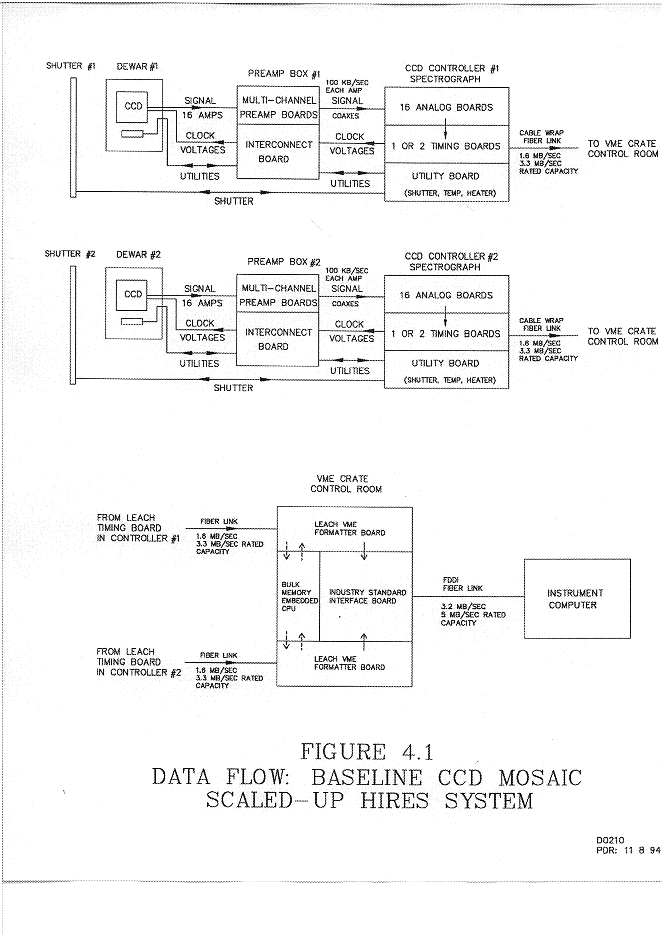
case, the overall system block diagram is similar, and is shown in Figure 4.1, which conservatively assumes the fallback design. If the second-generation system is used, as
planned, then the number of analog boards needed per controller is half that shown in Figure 4.1.
4.2.1 System Block Diagram, Data Rates Per Channel and in Total
The major components of the CCD controller system are illustrated in Figure 4.1, as
follows:
a) Preamplifier boxes (2, one per dewar)
The preamplifier boxes (sometimes referred to as the "saddlebags") are mounted
astride each dewar as close as possible to the detectors. These boxes serve two functions.
Signal cables coming out of each amplifier run into the multi-channel preamp boards (see
Section 4.2.2 below) and are thence routed to the amplifiers on the analog boards of the
CCD Controller. Incoming clock signals and bias voltages also enter on ribbon cables
from the CCD Controller. These are interfaced to input pins on the detectors via "interconnect boards".
b) CCD Controllers (2, one per dewar):
Each CCD Controller chassis is located within an electrically-shielded, thermallyinsulated, and actively-cooled enclosure located in close proximity to each dewar. These
chassis each contain analog, timing, and utility boards mounted on a standard 3U-format
VME backplane. (Although the backplane follows the VME bus mechanical standard, the
signal assignments on the backplane correspond to UCSD's custom bus specification and
not to the standard VME bus signal specification.) In the current UCSD controller design,
each readout amplifier reads out into its own analog board, while in the second-generation
design each analog board will service two readout amplifiers. The output from up to 16
single-channel (or 8 dual-channel) analog boards can in principle be multiplexed through
a single UCSD timing board (see Section 4.2.3.5 below), although under the current design
there is a 0.6 µsec-per-pixel overhead for each amplifier multiplexed; hence the
desirability perhaps of using two timing boards per CCD controller. The utility board is
used for shutter and dewar temperature and might also be used for liquid nitrogen level-sensing and control as was done in the HIRES system.
c) VME Crate (in Control Room):
Each timing board in the CCD Controller transmits its data directly to the Control
Room via a pair of fiber-optic cables contained in the telescope cable wrap. The signals
are received there by an interface board, which is located inside the chassis known as the
"CCD VME Crate". In the HIRES system, this crate is located on the Nasmyth platform,
but we think it will be more straightforward and simpler to follow the model that was successfully used by LRIS and bring the signals directly down to the conveniently located
and thermally controlled environment of the Control Room.
Since the communications protocol used by the UCSD timing board does not correspond to any industry standard, the dual fiber cable pair from each timing board must be
received by an interface board, which converts the data stream to a format that can be
accepted by the Instrument Computer. This interface also performs pixel descrambling,
needed since the parallel readout of multiple amplifiers results in a geometrically interleaved data stream.
The exact nature of this interface is TBD and depends on evaluation of alternative
interfaces that are or will become available (e.g., the "UCSD to SCSI interface" proposed
by McCarthy and Stubbs, or the UCSD's S-bus interface that will be part of the secondgeneration UCSD system). In developing the budget, we have assumed the use of UCSD's
existing DSP-based VME interface board, although we hope to find something better and
less expensive by 1996 when it will be needed. The use of UCSD's VME board requires a
separate 6U-format VME chassis (hence the name "VME Crate"). The VME Crate connects to the Instrument Computer via a high-speed industry-standard interface (e.g.,
FDDI) feeding a second high-speed fiber link.
The second-generation UCSD system will provide a choice between using either a
VME interface board or an S-bus interface board to receive the data via the fiber-optic cable from the UCSD timing board. If UCSD's S-bus interface becomes available in time
for DEIMOS, and if the instrument computers selected for DEIMOS have S-bus slots (as
would be the case if Sun workstations were chosen), then this interface could provide a
path for connecting the UCSD CCD Controller timing board directly to the Instrument
Computer, thus eliminating the CCD VME Crate in the Control Room. There are both
advantages and disadvantages to eliminating the CCD VME Crate. The major advantage
is a significant reduction in expensive hardware and an overall simplification of the system
architecture. The disadvantages include losing the processor in the VME Crate (thus
shifting more of the processing load onto the Instrument Computer) and losing much of
the software inheritance from the HIRES and LRIS CCD systems. These trade-offs will
be examined more thoroughly if and when it appears that this S-bus interface board will be
available in time to be used for DEIMOS.
Figure 4.1 also provides the relevant data rates per channel. A data rate of 100 KB/sec
per amplifier (or 50 kilopixel/sec per amplifier, since each pixel yields 2 bytes of data) is
shown, which is in-between our goal of 200 KB/sec and the specification of 66 KB/sec.
To meet the goal, the various rates shown on Figure 4.1 should be increased by a factor of
2. This increase in rate does not otherwise change the diagram, except that a second FDDI
board, or alternative interface, will likely be required between the VME Crate and the
Instrument Computer.
Additional details and data rates are considered in Section 9.2.
4.2.2 Preamplifiers
The current plan is to use the same-style external preamplifier boards as are used in
HIRES and at Lick. These are based on an amplifier design by Janesick, which has been
in use for over a decade. While this design has worked well, some improvements are
needed to optimize its use with dewars that provide AC coupling between the CCD output
amplifier and the preamp (see 4.2.2.1 below). For DEIMOS, since the preamp board is
exposed to dome air, we may need to consider using military-grade components on the
preamp board in order to meet the gain stability requirements.
In the existing HIRES implementation, each preamplifier board contains two independent channels. Depending upon mechanical packaging constraints imposed by DEIMOS,
it may prove necessary to lay out a new version of this board containing more channels.
To minimize noise, it is vital that these preamplifiers be mounted as close as possible to
the dewar, such that the length of coax cable from the dewar connector to the preamp input
is no longer than 3-4 inches. The preamplifier boards must be housed in a well-shielded
metal enclosure that is coupled directly to the side of the dewar. Proper grounding and
shielding is critical, since the signal levels from the CCD are extremely low-level and susceptible to noise pickup. It is also vital that the +15 and -15 DC volts power supplied to
these external preamps be extremely stable and free of significant noise. Thus, the supplies for these preamps must be very well regulated and heavily filtered. In the HIRES
and MOS systems, we have employed separate Pi-filter networks for each preamp supply.
4.2.2.1 DC Restoration
Since the DEIMOS dewar will most likely follow the standard Lick (and HIRES)
dewar design which employs a protective AC coupling capacitor within the dewar, an
active DC restoration mechanism will be provided as part of the preamplifier to insure that
this coupling capacitor is properly discharged during each pixel time. In the initial HIRES
implementation, this coupling capacitor (whose primary purpose is to protect the CCD
output amplifier from accidental damage resulting from unexpected transients that originate outside the dewar) was found to be a significant source of residual signal. Bright features in the imaging area resulted in residual signal that was noticeably present in the
overscan region and which complicated the use of the overscan pixel data for compensation of row-to-row baseline drifts. Such features would also result in low-level residual
signal contaminating adjacent imaging areas.
A prototype version of this DC restoration modification to the preamplifier has been
assembled and tested (see Figure 4.2). To insure that the TTL logic level which activates
the DC restore mechanism does not create ground loops which would introduce noise into
the preamp, this level is received via an HPCL optical isolator. When tested with Te tronix 2K x 2K CCDs, it effectively eliminates residual signal bleed-through into the overscan region without increasing the readout noise of the system. However, we have had
mixed results with this modification when used with other types of CCDs, such as the
Loral and Orbit 2K x 2K devices, where this modification has increased the readout noise.
It is suspected that for these devices we are discharging the coupling capacitor too rapidly
and that a small series resistance in the clamping circuit is probably needed. We anticipate
that further design iterations of this DC restoration circuit will be needed to optimize its
function with whatever CCDs are ultimately used for DEIMOS.
4.2.2.2 Cabling
All of the video signals from the dewar to the UCSD CCD electronics chassis will be
carried on coaxial cables. While these video signals will penetrate the dewar wall via the
same vacuum-tight multi-pin MS connector that is used to carry the clock waveforms and
bias voltages, each video signal pin will be surrounded by ground pins to insure adequate
shielding and isolation from the non-video signals in the connector. The coaxial cable
conductor will be soldered directly to the pin carrying the video signal, and the ground
braid connected directly to the surrounding ground pins. This technique has proved successful on HIRES and on all dewars used at Lick. We have not used separate BNC connectors for the video signals because we have been unable to find versions of these
connectors which are vacuum-tight. Given the large number of video, clock waveform,
and bias voltages required to support the DEIMOS mosaic, we anticipate that several such
large multi-pin MS connectors will be needed on each dewar.
As noted earlier, the preamplifiers will be located as close as possible to the dewar to
minimize the cable length to the input of the preamplifier. Similarly, the UCSD CCD electronics chassis will be located as close as practical to the preamplifier enclosure, although
for these cables lengths of several feet are quite acceptable.
The bias voltages and clock driver signals originate from the UCSD analog boards via
37-wire flat ribbon cables terminated in DB37 connectors. Approximately half of the
wires in these cables are grounds. Based on recent tests conducted at Lick, some small
improvement in readout noise might be achieved if each ribbon cable were encased inside
a large tubular ground braid. Inside a well shielded enclosure near the dewar, these ribbon
cables will terminate on a dewar interconnect board, which allows re-arrangement of the
signal lines into cabling that attaches directly to the vacuum-tight dewar connector. This
interconnect board may also contain analog switches which can be used to electrically isolate the CCD from the UCSD chassis without the need to disconnect cables. Such isolation
was needed in the Keck I UCSD system to insure that the CCD was protected from
momentary power-up and power-down transients from the UCSD analog boards. Such
isolation may be unnecessary in the second-generation UCSD system.
For the DEIMOS mosaics, the potential number of bias voltage, clock driver, and
video lines which might penetrate the dewar wall could be quite large, as might be the size
of the dewar interconnect board. What is unknown is which signals must be supplied
independently to each quadrant of each chip, and which signals can be shared. There are
potential trade-offs between cross-talk, readout noise, readout modes, and cabling complexity that may require a significant amount of testing to resolve. At present, it is
expected that the bias voltages will be independently provided to each amplifier of each
chip in the mosaic. Whether the clock signals also need to be supplied using independent
drivers and wires, or whether the corresponding clocks can be shared between some or all
of the chips of the mosaic, depends on the results of various cross-talk and readout noise
tests.
4.2.2.3 Electronic Cross-Talk Tests
As noted, we need to check carefully that the multi-channel preamp boards provide
adequate inter-channel isolation, to insure that they are not a source of cross-talk between
amplifier channels. The multi-amplifier readout CCD cross-talk tests should be tried with
various configurations of signal routings, comparing two channels routed through the
same multi-channel preamp boards versus completely separate boards.
In addition, since the current preamplifier design is over a decade old, we should
investigate whether it can be improved by the use of more modern components which
might yield lower noise and better gain stability under temperature variation.
4.2.2.4 Other Risks
The staff of the UCO/Lick CCD Detector Lab does not yet have experience dealing
with mosaics of CCD chips within a common dewar. Aside from the various mechanical
challenges to be faced, there may be subtle electronic interactions that effect readout noise
and cross-talk and which are critically dependent on how the dewar is internally wired,
and how the wires are routed, packaged, and cross-connected at the dewar interconnect
board. The amount of testing time required to arrive at an optimal solution could be significant.
4.2.3 CCD Controllers
4.2.3.1 UCSD Controller
The current plan is to use UCSD CCD controllers for DEIMOS. HIRES and LRIS
used a first-generation UCSD model. UCSD is currently developing a second-generation
system which should be available in mid-1995 and which should provide significantly
higher readout rates than the existing system (see Table 4.1). If this new system is available in time and provides the expected gains in performance, we hope to migrate to that
system, building on the experience we have with the first-generation system. This is our
default plan. Otherwise, the fallback plan is simply to do a brute-force scaled up version
of the first-generation UCSD system that was used for HIRES. The UCSD CCD Controller
components were listed in Section 4.2.1.
UCSD plans to have its new controller working by mid-1995. We recently (10/28/94)
verified with Leach that he is still on schedule. Table 4.1, extracted from the paper presented by Leach at the 1994 IAU Meeting in the Hague, compares some of the important
characteristics of the old and new controllers.
4.2.3.2 Other CCD Controller Options
There are other CCD controllers in use or under development at other observatories.
These include:
Of these, probably only the ARCON Controller could be considered as a reasonable alternate to UCSD. All of the others are still in early stages of development or are not likely to
be available as finished printed-circuit boards. Even parts of the ARCON Controller are
available only in custom Speedwire board form, and our latest information is that it will
not be available in finished PC form for about two years. Nevertheless, we have evaluated
the ARCON Controller because the analog signal processing portion is reported to be well
designed, low-noise, and compactly packaged.
There are also a few commercial controllers available such as those from Pulse Instruments and Astromed, Ltd. However, their designs do not handle large mosaics with many
readout channels.
4.2.3.3 Justification of UCSD Controller
The UCSD Controller was selected for the Keck instruments because it was an available, working system long before any other controller. At Lick we now have years of
experience in programming, developing, debugging, and actual on-telescope use of the
current UCSD system. There are working systems on the Keck telescope (HIRES and
LRIS spectrographs) and on the Shane telescope (MOS dual-beam fiber-fed spectrograph). We are currently building another UCSD system to run our IR detector arrays
on Mt. Hamilton. We also have a close working relationship with Bob Leach, which has
proven very valuable in debugging and testing both hardware and software. In addition,
the existing UCSD system is in use at several other sites in Hawaii (i.e., CFHT and IFA),
as well as numerous other sites in the US and Europe. There is an organized users' group
and associated e-mail mailing list which allows UCSD users to communicate with each
other and with UCSD.
Although the existing UCSD system has some deficiencies in terms of its packaging
and power-up/power-down transients, neither of these has proved fatal, and both should be
addressed by the new UCSD Controller. For the HIRES Spectrograph at Keck and the
MOS Spectrograph at Lick, we have found that the existing UCSD system meets our current performance specifications with respect to both readout rate and readout noise. The
existing system also meets the readout noise requirements of DEIMOS, although it falls
short of our readout rate goal by more than a factor of three. The second-generation UCSD
system should satisfy the readout rate required by DEIMOS and should also result in a
more compact and efficient package for a CCD mosaic system.
While the new UCSD Controller will have some important differences, it will in many
respects be similar to the current system. In the new system the controlling DSP processor
will be faster, but it will be the same type of device, and our programming skills and tools
are already in place for these devices. The details of the clocking waveforms will be different, but the general approach to creating waveforms from memory tables will remain
the same. Equally important, the existing CCD Controller support code that runs in the
VME Crate and the host computer will, in most cases, need little modification to work
with the new UCSD Controller. All of these points demonstrate that the adoption of the
new UCSD system will be an evolutionary change rather than a revolutionary one. The
infrastructure already exists at Lick (and Keck) to work with these systems. Discarding
that infrastructure in favor of a new system would be very costly in dollars and time and
could be justified only if there was an overwhelming advantage.
That overwhelming advantage does not appear to exist. As indicated in the previous
section, the ARCON controller is the only other system comparable to the UCSD system.
It is a proven system, working now on CTIO telescopes. However, it is a very different
system from the UCSD Controller. An entirely new infrastructure would have to be developed to support the ARCON system. But there is no obvious advantage in cost, complexity, data quality, or scientific productivity that could justify the switch. In fact, in most
parameters of interest to DEIMOS (primarily readout speed and ability to handle many
readout channels), the systems are comparable.
In the previous paragraph we said that discarding our UCSD Controller infrastructure
would be costly. That is an over-simplification since we could not actually discard it. We
already have UCSD Controllers running that must be maintained and supported, so we
would have to add a new support infrastructure if we were to adopt a different controller.
This would be even more expensive both in immediate costs to DEIMOS and in terms of
long-term maintenance, support, and development. All of this expense and personnel
expertise would have to be duplicated at Lick and at Keck. None of this can be justified.
4.2.3.4 Keck Experience With UCSD
The Keck experience with UCSD has been mixed. In HIRES, the UCSD system has
performed well in terms of its reliability and readout noise. On the other hand, LRIS initially experienced significant problems with readout noise on their UCSD system. Some
of this difference is due to differences in cabling and dewar wiring between the HIRES
and LRIS systems. However, the HIRES UCSD system is located in a somewhat more
benign environment, inside a shielded and insulated compartment which is itself inside of
the larger, metal HIRES enclosure, while the LRIS UCSD Controller is in a much more
exposed and less adequately shielded location at Cassegrain focus. After investing additional effort in grounding and shielding, the readout noise performance of the LRIS UCSD
system has been significantly improved and is now close to that of HIRES.
The conclusion is that the UCSD systems are relatively sensitive to noise pickup from
the environment and that careful attention must be given to the design of the shielding and
grounding of the enclosure in which they are to be contained.
4.2.3.5 Risks In Expanding UCSD To 32 Amplifier System
In the default plan, there would be a separate UCSD CCD Controller chassis for each
dewar. Since each of these chassis must provide for readout of 16 amplifiers, each would
require 8 dual-channel analog boards. In addition, each chassis would require one timing
board for overall control and data transmission, and one utility board to control auxiliary
dewar functions such as control of the shutter, dewar temperature, and liquid nitrogen levels. Thus, a total of 10 boards would be needed for each Controller, and these would plug
into a 10-slot 3U format VME backplane. This number of UCSD boards per Controller is
more than twice the number currently used in the HIRES and LRIS Controllers (4 in each:
1 timing, 1 utility, 2 analog) and not quite twice that used in MOS system at Lick (6
boards: 1 timing, 2 utility, 4 analog).
While a 10-slot VME backplane should not in itself present any technical problems,
the longer backplane and larger number of boards (and resultant heavier loading of signals
on the bus) places more stringent requirements on the bus driver circuitry employed on the
timing, utility, and analog boards. While we have been able to operate our existing UCSD
Controller chassis without bus terminators on the backplane, the longer backplane and
higher board count for 16 amplifiers may make these necessary, and this in turn will
impact the bus driver circuitry. In addition, since the second-generation UCSD system will
run 2.5 times faster than the current system (40 nsec per instruction versus 100 nsec), the
driver circuits and backplane will need to support higher-speed signals. Meeting these
requirements is well within the capabilities of the VME backplane and of currently available bus-driver chips, and we are confident that the second-generation UCSD system
should be able to meet them. However, it is prudent to note that these requirements are
several times more difficult to meet than those faced by the current UCSD system.
If the second-generation UCSD system does not become available on schedule, then
similar concerns regarding bus length and bus loading apply when scaling up the current
UCSD system to support 16 amplifiers per Controller. Since the existing UCSD system
supports only a single amplifier per analog board, 16 of these boards would be needed per
Controller, and an 18-slot 3U format VME backplane would be required, since 2 additional slots are required for the timing and utility boards. This is only 3 slots less than the
maximum length backplane (21 slots) and is thus pushing the bus length close to its theoretical limit. While the existing UCSD system should in theory be able to support this
number of analog boards per chassis, we have never had enough analog boards to actually
test this, nor are we aware of any other sites which have. Should this prove to be a problem, the second-level fallback plan would require having two UCSD CCD Controller
backplanes per dewar, with each such backplane having 10 boards/slots. This would also
double the number of VME interface boards required in the CCD VME crate in the control
room. Finally, it would increase the volume, weight, and heat dissipation of the UCSD
chassis that are mounted within the spectrograph. All of these impacts would be expensive, and it is worth considerable effort to avoid them.
4.2.4 VME Crate (Control Room)
Depending upon the availability and usability of UCSD's S-bus interface board for the
second-generation UCSD system, the CCD VME Crate might be eliminated from the overall system, providing a significant savings in cost.
If the S-bus interface option does not prove viable, then we will proceed with building
the VME crate as illustrated in Figure 4.1. While the precise components are not yet
known, they will consist of:
Current Planned Typical readout time (21+2 x n) µsec/pixel 18 µsec/pixel Fastest readout time for N=8 readouts 26 µsec 3.2 µsec Readout noise 0.7 ADU A/D converter 16-bits, 10 µsec convert 16-bits, 2 µsec convert (19-bit w/auto- scaling) Selectable gain 2 choices 4 choices Timing sequencer DSP56001 100nsec/instruc. DSP56005 40 nsec/instruc. CCD clock drivers per board 12, in 0.1 V steps 14, in 0.01 V steps Board size 10 x 26 mm 10 x 23 mm Power dissipation for two readouts 23 watts 18 watts Boards needed for four readouts 6 4 Practical maximum number of readouts 8 16 Computer interfaces VME VME, S-bus
| Read out CCDs: | Goal = 42 sec | Spec = 120 sec | |
| Transfer data from UCSD timing board to VME crate memory: | 0 sec * | ||
| Transfer data from VME crate memory to instrument computer: | 0 sec * | ||
| De-interleave pixel data and stitch together into mosaic: | 0 sec * | ||
| Display raw image(s) on monitor(s): | 0 sec * | ||
| Write raw image(s) to disk: | Goal = 13 sec | Spec = 20 sec | |
| Total time: | Goal = 55 sec | Spec = 140 sec |
The CCD readout time goal of 42 sec corresponds to a readout rate of 100 kilopixels/ second/amplifier, or 10-µsec/pixel/amplifier, while the specification of 120 seconds corresponds to a 33 kilopixel/sec/amp rate, which is comparable to the existing HIRES and LRIS systems. The intervening processing steps between CCD readout and writing to disk are assigned zero time (and marked with *) to indicate that these operations are overlapped with the CCD readout using a similar data transmission and processing pipeline to that used for HIRES and LRIS.
Writing of the image(s) to disk is not overlapped with the CCD readout because the
image(s) must first be completely de-interleaved and stitched together before disk writing
operations can be initiated. The disk write time goal of 13 seconds assumes a sustained
disk write rate of 20 megabytes/second, while the specification assumes a more conservative rate of 13 MB/sec. Either of these implies the use of RAID disk technology. The
exact format in which the image(s) will be written to disk is TBD. Initial plans call for
writing the image from each CCD as a separate FITS file, rather than writing the 128
megabytes of data from each dewar as a single monolithic file.
GO TO CHAPTER 5