3.1 Overview of DEIMOS Focal Plane Detectors
3.1.1 Main CCD Mosaic
The CCD mosaic, shown in Figure 1.6, represents an aggregate 8K x 8K 15µ-pixel detector array. No CCD manufacturer can fabricate a single CCD of this size. Therefore it must be built up from a mosaic of smaller devices. Such an array could, in principle, be built from a mosaic of four 4K x 4K CCDs. While this might make the design of the dewar and its CCD adjustments somewhat simpler, it represents a significant risk in our efforts to obtain the CCDs and would drive the CCD cost up significantly. In view of the level of success by several manufacturers in producing 2K x 2K CCDs, our judgment is that they can probably make 2K x 4K CCDs with reasonable yield and at reasonable cost. Therefore, this size was selected for the DEIMOS array. Given this size, a number of other requirements result. First the CCDs must be closely buttable on three sides. This means there will be only one serial register per CCD. With an output amplifier at each end of the serial register, we can read out the entire CCD in 4.2p seconds, where p is the pixel time in microseconds. We hope to achieve a pixel rate of 100K/sec, or 42 seconds for the entire CCD. In addition, we expect to read all output channels from all of the CCDs in parallel, so 42 seconds will also be the time to read the entire mosaic.
3.1.2 Flexure Control CCDs
If flexure control (FC) is implemented, CCDs will be used to compensate for spectrograph flexure during a spectroscopic exposure. There will be two flexure control CCDs
for each mosaic. They will be fed with an arc spectrum (or perhaps an etalon) through two
fibers near the ends of each slitmask. To cover a large enough portion of the spectrum, the
CCDs should be as large as possible. The CCDs will be fabricated by Orbit Semiconductor on the same wafers used to produce 2K x 4K CCDs. We selected a 600 x 1200 15µ
pixel CCD format, which is very close to the largest CCD that will fit onto the wafer. The
FC CCDs will have a single serial register along one of the long sides of the device and
will operate in frame transfer mode. The opposite side of the device will have no structures or pinouts and therefore can be positioned close to the main mosaic detector. The FC CCDs will not be thinned.
3.2 Detailed Specifications For Individual Mosaic CCDs
3.2.1 Summary of Performance Requirements
The following table lists the performance requirements for the DEIMOS CCDs.
| Function | Value |
|---|---|
| CCD detector | 2048 x 4096 3-side buttable |
| CCD type | Thinned, back-illuminated |
| Nominal pixel size | 15 µ |
| Full mosaic array each camera | 2 x 4 array |
| Size of full mosaic | 8192 x 8192 px, 4.84-in. x 4.96-in. |
| Mosaic packaging goals | Single gap <100 µ in l; < 1 mm along slit |
| Surface treatment | AR coated, red optimized |
| QE optimization (backside passivation) | Coating, implant or UV flood (least desired) |
| Detector flatness | <10 m peak to valley over full array |
| Readout characteristics | 2 amplifiers per detector, all multiplexed |
| Total amplifiers, full mosaic | 32 |
| Total readout time | <120 s for both cameras; 42 s goal |
| Full well (integration and clocking) | >150,000 e- |
| Charge transfer efficiency (CTE) | >0.999995 per pixel for 1600 e- signals |
| Readout noise | <5e- |
| Dark current | <0.001 e- s-1 |
| Linearity | <0.5% deviation up to 50% of full well |
| RQE | >90% somewhere in range 0.5-0.7 µ >50% at 0.9 µ |
| Fringing | <10% peak to peak at any l |
3.2.2 Detailed Layout
The detailed layout will to some extent be determined by the supplier of the CCDs. Suppliers are free to vary the detailed layout within the constraints defined in Table 3.1. Some parameters, like the 15 µ pixel size, are matched to the optical performance of the spectrograph so we do not want to vary them. Other parameters, like the total number of rows or columns, could be varied a little without seriously affecting the science capabilities of the instrument. We want to give manufacturers as much leeway as possible, since small changes could make a large difference in cost.
3.2.3 Specific Performance Numbers and Justifications
1) Readout noise
Our goal, as stated in Table 3.1 is <5e- readout noise. Note that we have not specified a readout speed. We will read out as fast as possible, within the capabilities of the controller hardware, while keeping within the 5e- limit and maintaining other important readout parameters (such as CTE). As stated in Section 3.1.2, we hope to achieve a readout rate of 100 Kpixels/s. The 5e- readout noise limit is set by the fact that the sky noise in the darkest parts of the spectrum will be 10e- per pixel in a 2000 sec exposure at highest dispersion (see Figure 1.1).
2) RQE and AR coatings
Since the mirrors of Keck II will be silvered, DEIMOS is optimized for the red spectral region. Our RQE specifications are based on demonstrated capabilities for thin devices operating in the 0.5-0.9 µ range using multi-layer antireflection coatings. Even without multilayer coatings we should be able to achieve >80% RQE somewhere in the range 0.5-0.7 µ, and >40% at 0.9 µ. Section 3.4.3 describes investigative work with deep-depletion CCDs which may result in even better red response.
3) Backside passivation
The precise method of backside passivation will depend on the CCD supplier. For instance, Lincoln Labs and SITe utilize a boron implant with anneal. Foundry-produced CCDs on the other hand (such as those from Orbit) may have no built-in passivation and may require UV flooding. Because UV flooding is not permanent, we would like to avoid it if possible. Section 3.4.3 describes work we are doing to address backside passivation for foundry-produced CCDs. On the timescale that we may expect to obtain science-grade CCDs, delta-doping of our Orbit CCDs at JPL may also be possible.
4) Fringing
The calibration and removal of the effects of fringing in thinned CCDs is one of the most difficult data reduction problems today. The problems are made worse if instrument flexure makes the fringe pattern unstable, if the amplitude of the fringes is large, or if the physical peak-to-peak distance between fringes is small. Our specifications define a maximum fringe amplitude since this is an aspect we can hope to control. The peak-to-peak distance between fringes is determined by the detailed characteristics of the thin CCD membrane and is much harder to control. Given sufficient funding and time, we may be able to selectively pick science grade CCDs with particularly large peak-to-peak fringe distances, but it is not obvious at this time that such a selection will be possible.
We will be addressing the fringing problem in three ways. First, a good red-optimized AR coating can help to reduce the amplitude of the interference fringes. This will be done. Second, we are investigating an active Flexure Control system which would help to dynamically remove instrumental flexure and improve fringe pattern stability. Finally, we are doing experimental work with Orbit (see Section 3.4.3) on deep-depletion CCDs which could help to reduce fringe amplitude.
5) Flatness
The flatness requirement is set by the speed and resolution of the cameras and the size of the CCD pixels. A variation of 5 µ causes an image defocus of 2.5 µ, small compared to the nominal image FWHM of 17 µ. Normal silicon wafers are flat to better than 1 µ, and, if the CCD is attached to a solid substrate before thinning, this level of flatness is easy to maintain. We have measured the flatness of Reticon-thinned CCDs and Lesser-thinned CCDs, and both meet our flatness requirements. We know how these CCDs are mounted and thinned, so we are confident that we can achieve similar results with Lick-thinned CCDs. Lincoln Lab personnel have also demonstrated the capability to achieve our flatness requirement.
6) Full Well
The full well specification is a typical charge handling capacity for 15 µ pixels. Given the high amplifier gain typically used during readout (~ 1 e-/DN) and the dynamic range of the readout ADU (16 bits), less than half of the full well is typically used. The additional charge handling capacity helps to insure that non-linear response near pixel full-well does not effect the data.
7) CTE
The CTE specification is based on the desire to minimize smearing of the image during readout. A parallel CTE of 0.999995 would result in about 2% smearing of the charge in the last row of the array, and the same CTE in the serial register would result in about 0.5% smearing of the charge in the last column (using both amplifiers).
8) Dark Current
The dark current specification (< 1 e- in 1000 s) is typical of current CCDs and is low enough that the contribution to the noise from the dark current will still be small, even for a 3-hour exposure.
9) Linearity
The linearity specification is typical of current CCDs and should not be a problem to achieve.
10) Other
The DEIMOS CCDs do not need frame-transfer capability. Whether or not the CCDs selected will have frame transfer capability will depend on the supplier selected. Orbit 2Kx 4K CCDs do not have frame transfer. Lincoln Labs CCDs will. Skipper amplifiers are not planned for the DEIMOS CCDs. In fact, with the improving performance of non-skipper amplifiers the reasons for skipper amplifiers are quickly disappearing. The CCDs will be capable of on-chip binning in both rows and columns. MPP implants may not be used to suppress dark if the devices come from Lincoln. In this case dynamic suppression of the dark will be used.
3.3 Specifications for the Assembled Mosaic
The basic alignment tolerances for the CCD chips in a mosaic are as follows:
In general, the surface tolerance is tighter and more important scientifically than the
rotation and alignment tolerances. Also, we expect that the surface alignments are more
likely to change significantly when the dewar is cooled. These considerations lead to the
following basic alignment scheme:
1) Adjust rotation and x, y alignments using screw adjustments while the dewar is
warm. With fine-thread (#0-80) screws, a 5 degree wrench rotation equals 5 µ. We think this
will just be adequate to achieve the rotation tolerance and will be more than adequate
to align in x and y.
2) Make coarse alignments in tip, tilt, and piston using screw adjustments while the
dewar is warm. Fine movable stages with feedthroughs outside the dewar will be used
to tune the surface while the CCD is cold.
It is a requirement that individual chips in the mosaic can be separately removed and
replaced.
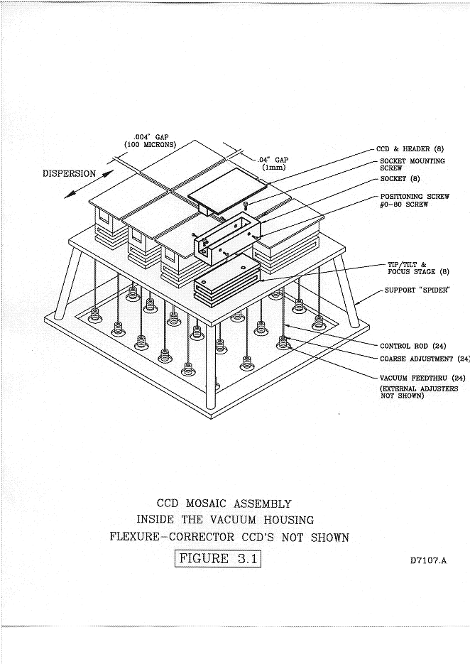
Figure 3.1 shows a schematic of the assembly procedure for the 2 by 4 mosaic of
CCDs. Before beginning, the 8 CCDs to be mosaiced are first measured. Each header
(i.e., substrate) and CCD will be measured so that its holding hardware can be coarsely
positioned. The headers are made of aluminum nitride, and each CCD is bonded to the top
surface. The CCD will not extend past the edge of the header. Each header has a rib along
its back surface. The rib is about 0.2" by 0.2" by almost the full length of the header. This
can be seen in the schematic. The rib fits loosely into a socket. The final "coarse" height
of each CCD will be determined by the machined top surface of each socket.
Rotational alignment of each CCD will be accomplished by turning fine-thread screws
(#0-80) in the socket. We will use special small hand tools. One of the two long edges of
the 3-edge-buttable CCD will be used to check angular alignment. The sawing process
that makes this edge will be accurate to 1/2 pixel in 8192 pixels, which is the key that
allows us to meet the tolerance. A microscope will be used in a milling machine to look at
the edge. We have done this many times. We expect to have to survey the cut edge
because we cannot see pixels on the front surface since these CCDs are back-side illuminated. However, we will also investigate whether an infra-red TV mounted on the microscope can see pixels. This has the potential to be more accurate. Small fine-thread screws
will then be used to position the CCDs end-wise so that the gap between butted CCDs is
less than 100 µ (0.004"). The gaps in the other direction will be approximately 1 mm
(0.04"). These large gaps must line up with the webs in the slitmask in the instrument
focal plane to within 0.1 mm. The slit-mask webs will "hide" in these 1 mm gaps. The
focal reduction reduces the 0.2" thick webs to (0.2"x15"/86.5"=0.034"), or 0.8 mm wide
shadows. Figure 1.6 shows the mosaic and gaps in more detail.
The 8 individual sockets are attached to 8 movable stages. The purpose of these stages
is to tip, tilt, and piston in the z direction (parallel to the optical axis of the camera). The
stages are mounted to the top of a thermal standoff structure called a "spider". This structure is made of thin-wall stainless steel tubing welded to upper and lower stainless steel
mounting plates. This can be seen in Figure 3.1. The heat flow through this spider is less
than 500 milli-watts.
Under the weight of the CCDs, mounting sockets, and stages, the "spider" flexes in the
plane of the detector by less than 0.000 02" (0.5 µ). We have assumed the weight of these
items is approximately the same as a 4" by 4" aluminum plate that is 0.5" thick. This
motion occurs twice per revolution of the instrument and motion is well within specifications. The natural frequency is 800 Hz.
Connecting links attach the tip, tilt, and focus stages to vacuum feedthroughs. Each
stage will have 3 vacuum feedthroughs. There are coarse adjusting screws below these
stages to bring all CCDs into a common plane to within a tolerance of 0.002" (50 µ). The
microscope is used for this. It has a depth of focus of 0.001". There are 3 coarse adjusting
screws per CCD, or 24 total adjustments. These adjustments will be made in a clean room,
probably in the CCD Lab at UCSC.
The coarse adjusting screws attach to the vacuum feedthroughs and are accessible outside the vacuum dewar for what we refer to as the "cold adjustments". These adjustments
will be made after the vacuum chamber is sealed and evacuated and the CCDs are cooled
to approximately -120 C. We will be using images to accomplish the final adjustments.
At this time, the z-axis spec is approximately 0.000 2" (5 µ, or 1/3 of a pixel width).
We also plan to experiment with an interferometer to try to simplify the final alignment procedure. Other ideas will be solicited, too.
The flexure-correcting CCDs seen in Figure 1.6 will have no "cold adjustments". The
initial locating will be sufficient (30 µ of z-axis error is tolerable.)
Electrical wires will be connected to each CCD before it is inserted into its socket.
This will avoid moving the CCD once it is aligned. The wires will terminate in a strip connector which fits into a ZIF (Zero Insertion Force) socket mounted inside the dewar. The
wires from the mating ZIF connector then lead to hermetic connectors.
The hermetic connectors are about 2" in diameter, which includes the external connector. Each dewar will have up to 10 of these large 61-pin Bendix connectors. The preamplifier boards must be mounted within 3" of these connectors. We have tried unsuccessfully to increase this distance. The major impact of this requirement is that the dewar vacuum housing will have connectors and pre-amp boxes mounted on all of its exterior
surfaces. This is not a problem but it is a lot of parts. If we find that it is possible to reduce
the number of connectors and pre-amp cards from 10 per dewar this will simplify the
dewar housing.
CCD Mosaic Summary:
The mounting and alignment requirements of the CCDs in the assembled mosaic
imply additional dimensional specifications for the individual CCDs. These specifications describe the tolerances for alignment of each CCD on its substrate, which in turn is
held by the mosaic mounting stage. The specifications will undergo some refinement as
the detailed design for the mosaic mounting is developed. The following table summarizes
the present specifications.
3.4 Acquisition Plan for Individual CCDs
3.4.1 Overall Plan: SSC and KCCDWG Activities
To address the task of acquiring CCDs for Keck Observatory instrumentation (HIRES,
LRIS, and DEIMOS) the Keck Science Steering Committee (SSC) established the Keck
CCD Working Group (KCCDWG). The members of the KCCDWG have been:
Chris Stubbs has recently relocated to the University of Washington and has resigned from
the KCCDWG. However, all decisions and findings so far by the KCCDWG related to the
DEIMOS CCDs have included Chris.
It has been the opinion of the members of the KCCDWG that Keck must take an active
role in the development of the CCDs needed by Keck Observatory. This opinion has been
backed by the SSC by statements and funding. With regard to the DEIMOS project, the
KCCDWG members have undertaken several tasks. First, a set of detailed specifications
was developed for the CCDs required for DEIMOS. Then a letter was sent to the following CCD manufacturers asking for budget estimates, development timescales, and fabrication concerns:
Based on the responses received and the current experiences and knowledge of
KCCDWG members it was the consensus of the KCCDWG and the SSC that we should
pursue further work at Lincoln, Orbit, and Loral. EEV was judged to be too expensive
(>$200K per CCD). Although Reticon pricing was attractive, they are more than 2 years
behind in their program to develop a thinned 2Kx2K CCD, so they were judged to be too
risky. The largest device Sarnoff could make had only 76% of the area of the 2Kx4K
CCD we require, and their development costs were high (>$800K). SITe indicated they
could not meet our flatness requirements.
At the time the KCCDWG was formed (early 1993), Lick had already been talking to
Orbit Semiconductor about a collaborative effort to develop scientific CCDs. With funding from Keck, UCSC, and the University of Hawaii we began our first wafer run at Orbit.
This activity was proceeding at the same time the specifications for the DEIMOS CCDs
were being developed, so we included a 2Kx4K 3-side buttable CCD in the first wafer run.
This first wafer run proved that Orbit could make high quality CCDs.
Following the review of CCD manufacturers by the KCCDWG, the SSC authorized
funding for further work at Orbit and Loral, and for additional investigation into Lincoln
Labs. The funds for Loral covered a single wafer run at their Newport Beach facility. But
since this facility is closing down, it was decided to reserve these funds until the situation
at Loral stabilizes.
3.4.2 Lincoln Labs Work
1) Consortium
To investigate Lincoln Labs further, members of the KCCDWG made a site visit to
Lincoln. The report on that site visit is included as Appendix D. As a result of the visit it
was concluded that further work at Lincoln should be funded. However, the initial phase
of development (usually referred to as Non-Recurring Engineering, or NRE) was expected
to cost between $0.5M and $0.6M. To lessen the cost to Keck it was decided to try to
develop a consortium to fund the NRE phase of the work. The consortium is headed by
Gerry Luppino of the University of Hawaii. Consortium members include:
Consortium members will fund equal shares of about $100K. These funds do not
come from the DEIMOS budget.
2) NRE phase
The NRE phase of the work at Lincoln will include the following:
It is expected that each consortium member will receive at least one working, thinned
CCD for evaluation. The complete NRE phase is expected to take about one year, and is
expected to begin in the first quarter of 1995.
The 3-side buttable package (header) for the consortium CCD will not be supplied by
Lincoln. This package will be designed by Lick engineers in collaboration with Lincoln
personnel and fabricated in the Lick shops.
3) Production phase
If the NRE phase of the work proves successful, then the SSC will have the option to
proceed with a production phase at Lincoln. The cost per CCD at this stage may depend
on the total number of devices produced by Lincoln, and this will depend on decisions
made by the other consortium members. However, the cost per finished, science-grade
CCD is expected to be between $50K and $75K. We will need an absolute minimum of
16 devices (for two beams), and 24 would be better. So the total budget for production
phase CCDs is between (16 x $50k), or $0.8M and (24 x $75K), or $1.8M. Note that our
current budget includes $0.43M for a single beam, so we are just within the minimum
needed to secure a full array assuming the lowest cost per device.
3.4.3 Orbit Work
1) NRE phase
The funding provided by the SSC for the NRE phase at Orbit covers fabrication of a
new CCD mask set and three additional wafer runs. Lick was able to negotiate a very
favorable price for these wafer runs, based on our continued cooperative work with Orbit.
We are getting the three runs for a total cost of only $60,000. Three additional runs at the
same price are also possible. A new mask set is required because on the original mask set
we had one 2Kx4K CCD and two 2Kx2K CCDs. The new mask set will have two 2Kx4K
CCDs along with the FC CCDs. The objective of the wafer runs is to test whether or not
Orbit can produce good 2Kx4K CCDs with sufficiently high yield to make them economically feasible. Low yield was the one area in which our initial wafer runs were deficient.
We hope to achieve at least a 25% yield of working 2Kx4K CCDs, with a science-grade
yield of 10%.
To help defray some of the cost of the NRE effort at Orbit we have established Memoranda of Understandings with NRAO and the Observatory of Rome, Italy, in which they
will share in the results of these first runs. A similar agreement with a group at Yale is
pending. In return for a share of the devices, each group has paid $22K. This doesn't
cover our costs for the CCD design, mask fabrication, or testing and packaging, but it does
provide us with the funds to continue with additional wafer runs (see below).
The first of the three new wafer runs is now under way. We expect to have devices
from this run by mid-January. If we find no problems that indicate a design error or mask
fabrication flaw we will start the next two runs as soon as our testing is completed. We
should have all three runs completed by June 1995. At the end of the NRE phase Keck
should have around six good science-grade CCDs (assuming 10% science grade yield),
and a larger number of lower-grade devices. The science-grade devices will have to be
thinned (see below).
In addition to Keck SSC funded activities at Orbit, Lick is engaged in a number of
additional activities which may have a significant impact on the DEIMOS CCDs. First, we
are doing some experimental work with a new kind of silicon wafer which has a double
epitaxial layer. The first layer has a very high boron concentration and the second layer
has the normal epitaxial properties upon which the CCD structures are fabricated. When
thinned, the boron epi-layer acts as a natural etch-stop and, even more importantly, may
provide backside passivation properties similar to the boron-implant with laser anneal
technique. If this works, it will greatly simplify the fabrication of thinned, high QE CCDs.
At least one of our remaining $20K wafer runs, and funds from our MOUs, will be used to
test these new wafers. The boron wafers have already been purchased with funds from a
Lick NSF grant.
In a separate effort at Orbit, Lick is working with a group at the Lawrence Berkeley
Lab to test Orbit's capabilities in fabricating deep-depletion CCDs. These are CCDs made
on high-resistivity silicon. The high resistivity allows the potential wells of the pixels to
extend deeper into the silicon, thus increasing the effective thickness of the CCD. This
means that the CCD would not need to be thinned as much. Thinning would be easier,
and the resulting thicker CCD would be more robust. A thicker CCD also means a longer
path length for absorption of red photons, thus increasing red RQE while reducing fringing amplitude. We will use another of our $20K wafer runs to test the deep depletion
CCDs.
Finally, we have been exploring the possibility of testing Orbit's capabilities in making
P-channel CCDs. Most electronic devices are made with N-channel material because the
signal carriers are electrons. In P-channel material the signal carriers are holes, which
tend to move much more slowly. For this reason most CCDs are made with N-channel
material. However, Orbit has some other commercial interests in developing P-channel
technology, and if we pay for materials costs (which might include a new mask set at
around $22K) they may pay for the wafer run. We are still discussing the details with
Orbit. The advantage of P-channel CCDs is that no backside passivation is required since
the back surface will naturally repel the signal carriers (holes). Such CCDs should naturally have good blue response when thinned. The lower mobility of holes should not be a
problem at CCD operating speeds.
If both deep-depletion and P-channel CCDs work we may be able to combine them to
make a CCD with high RQE across the entire spectrum. This would be a very major
advance in the state-of-the-art in CCD fabrication. By the end of 1995 all of the Orbit
NRE activities should be complete, or near enough to completion, to permit us to judge
whether or not Orbit will be a viable choice for further CCD fabrication.
2) Production phase
If the yield of good 2Kx4K CCDs at Orbit is high enough then we can elect to proceed
with a production phase. Assuming a 50% loss in thinning, we will probably want about
24 science-grade CCDs (for a single mosaic plus spares). If we get six in the NRE phase
then we will need 18 more science-grade CCDs, or 5 runs. At the 100-wafer production
level (5 runs) each wafer will cost about $1600 to process. If the double epi-layer wafers
are used, that will add an additional $3300 per run. Therefore the budget for production at
Orbit would be about $176.5K for a single beam. All of these funds do not have to be
committed immediately, and if the thinning losses prove to be less than 50% then the number of runs could be reduced. However, the costs shown here are based on an initial commitment of at least 100 wafers. If we order wafers in smaller lots then the cost per wafer
goes up. The production phase would last about six months, with a new run coming off the
fab line on average about once every six weeks. Devices would be tested and mounted as
they came in. If two mosaics are produced, the cost per wafer may be reduced further so
the total cost would not double.
3) Thinning and Packaging
Any foundry-produced CCD (whether at Orbit or Loral) will have to be thinned and
mounted in a separate effort. There seem to be three options:
The first option is to contract with Mike Lesser to thin our CCDs. The KCCDWG felt
that this approach had several shortcomings. One serious shortcoming is the exceedingly
low success level Mike has had for many years. While he now claims a much improved
success rate this has yet to be convincingly demonstrated. Equally serious is the high cost
of thinning. At $15K per CCD the budget for thinning 12 CCDs (one mosaic plus spares)
would be $180K. The three-side buttable package is also a significant departure from his
previous thinning efforts, and would require some development effort and additional
expense (~$100K). The KCCDWG was also concerned about Mike's ability to deliver the
CCDs on time. As the world's only supplier of thinning services for Loral (and now
Orbit) CCDs, Mike must have a tremendous backlog of orders, and if he thins CCDs for
Gemini, the situation will only get worse. Despite all these concerns, Mike's operation
may still prove to be a viable option, and we are not ruling him out at this time.
It has recently come to light that Reticon may be willing to provide thinning services.
However, given their poor performance in attempting to produce a thinned 2Kx2K CCD,
this does not seem to be a good option at this time. Nevertheless, such situations are
highly personnel dependent, and if the situation at Reticon changes, they may become a
viable option.
The third option is in-house thinning. For some time there has been interest at Lick in
setting up a thinning facility. It has been our opinion that all of the necessary talent is
available close to the Santa Cruz campus in Silicon Valley. Furthermore, a detailed estimate of the costs suggests that the actual cost of thinning and packaging a CCD could be
as low as $5000 if yields are kept high. Given the interest at Lick and the availability of
facilities and skilled personnel, the SSC decided to fund some preliminary thinning work
at Lick Observatory. If we are successful at thinning and we can hold costs down, we will
have spent no more money than if we had contracted with Mike Lesser, and at the end of
the effort Lick and Keck would have a very valuable resource in the thinning lab. The
SSC has provided $0.1M for a one-year effort, and $20K for lab remodeling at Lick. To
hold costs down we are acquiring as much equipment as possible through corporate dona-
tions. We have been very successful with this type of effort so far. Also, to hold costs
down and to achieve rapid success we plan to do as little development work as possible,
opting instead to purchase expertise and technology that already exists. For instance, we
have hired Dr. Charles Hunt from UC Davis as a consultant to help us design our thinning
facility and procedures. Dr. Hunt was instrumental in setting up the Tektronix (now SITe)
CCD thinning facility. We are also working with packaging specialists to design and fabricate the three-side buttable package (header).
We hope to be able to demonstrate successful thinning and packaging of 2Kx4K CCDs
within one year. If we are successful, then in-house thinning of Orbit (or Loral) CCDs
becomes a realistic possibility. If we are not successful, then we can still elect to use Mike
Lesser (or Reticon) without any impact on the time schedule for DEIMOS. None of these
development activities are changed to the DEIMOS budget.
3.4.4 Other Possibilities
Although Keck is investing in Lincoln, Orbit, and possibly Loral, this does not preclude acquisition of the needed CCDs from other sources if they become available. For
instance, SITe is said to be working on a 2Kx4K 15m 3-side buttable CCD. SITe CCDs
are known to have some serious problems. It is our understanding that they are planning
to reduce the 200m p-p curvature seen in their 2Kx2K to around 100m in the 2Kx4K
device, but this is still 10 times worse than our specification and is a fatal flaw in any
mosaic used behind a fast camera. If SITe can produce a 2Kx4K CCD with acceptable
flatness and do it on a reasonable timescale (SITe's record here is not very good but may
be improving) then they may become a viable source.
3.4.5 Selection of CCD Path and Costs
All of the NRE efforts at Lincoln and Orbit and the thinning demonstration effort at
Lick should be completed by the end of 1995. At that time, the KCCDWG in conjunction
with the DEIMOS team will examine the results from those efforts, will re-evaluate other
options such as SITe, and will make a recommendation to the Keck SSC. Criteria for
selection will include:
The deadline for choice of CCD vendor for DEIMOS is the CCD/Detector CDR in May
1996.
At this time the total cost to produce CCDs for a single mosaic at Lincoln is at least
$400K, and the total cost to produce them at Orbit with Lick thinning is projected to be
about $300K. These costs do not include the development work at Lincoln, Orbit, or Lick,
which is being supported by Keck SSC and other funds. The current budget allocates
$433K for CCD acquisition (plus additional funds for making the mosaic). This seems
adequate for Orbit-produced CCDs but will cover the Lincoln costs only if we can obtain
the lowest projected cost for Lincoln devices. The Keck SSC has indicated in the past that
it may be willing to fund further CCD fabrication outside any particular instrument budget. However, further decisions await NRE developments.
3.4.6 Fallback CCD Plans
1) Options
The ideal fallback option would have no impact on the project schedule or budget, and
no impact on the science capabilities of the instrument. Such a fallback option does not
exist. One obvious fallback is to employ unthinned 2Kx4K CCDs in the mosaic. These
should be relatively easy to acquire. They could be produced by either Orbit or Loral. A
phosphor coating could be applied to the CCDs to give them some blue response. This
fallback plan could be implemented at almost any time. The timescale to produce 16 thick
science grade CCDs would be 6 months or less, assuming four wafer runs were started in
rapid succession. This option would impact the science capabilities of the instrument
because of the reduced RQE in the thick CCDs. However, the complete elimination of
fringing provides a slight offsetting advantage. On balance we are not enthusiastic about
this fall back position because it would still be costly yet leave us far from our final goals
in terms of QE. Also, it does not provide peak performance for single-object observers
who require only a 1x2 mosaic.
If we acquire some of the thinned CCDs we need, but not all, two other fallback positions may be possible. First, a single spectrograph beam could be used if we have enough
CCDs for only one mosaic. Second we could install fewer CCDs in each mosaic.
In the event that we do not have a full complement of CCDs at first light, it is our highest priority to provide high RQE and full spectrum coverage for single-object users. That
means a 1x2 mosaic of thinned CCDs for one beam. This seems well within the scope of
the existing budget of $433K for a single-beam spectrograph, given the cost estimates
above. As more devices become available at feasible cost, we will extend the mosaic
upward along the slit. Since total funds are scarce, we are inclined to bank any unspent
dollars rather than build an interim but still costly mosaic of thick CCDs.
2) Decision Time and Criteria
The decision on implementing any of these fallback plans will be made about midway
through the planned production phase, or January 1997.
A fallback plan would be chosen and implemented only if it appeared likely that the
selected production phase was not going to produce the needed CCDs, or was going to be
significantly delayed, or run significantly over budget.
3.5 Acquisition Plan for the FC CCDs
The FC CCDs will be produced by Orbit Semiconductor. These CCDs will be fabricated on the same wafers as the 2Kx4K CCDs during the NRE phase at Orbit. These
CCDs are relatively small, so we should have a sufficient number of high quality devices
to choose from in the NRE wafers. We will need four FC CCDs in the instrument, with at
least one backup device.
These CCDs do not have demanding requirements. They will be thick. Split vertical
clocks will be used to operate the devices in frame-transfer mode, which will allow them
to be read out repeatedly, and without a shutter, during a single exposure on the main
mosaic. There is no additional fabrication cost for the FC CCDs. There is a small cost
associated with testing, dicing, and mounting the CCDs in suitable packages (~$200 per
CCD). Details of the mounting are described in Section 3.3.
3.6 UV Flooding
Loss of liquid nitrogen coolant for whatever reason might require ultraviolet flooding
of the CCD mosaic before re-cooling. (HIRES uses a Tektronix 2048 x 2048 CCD which
does not need to be UV flooded.) Our procedure at Lick is to move the dewar to a lab
where a UV lamp is positioned directly over the vacuum window and then the detector is
cooled. The UV lamp is then turned off and the dewar returned to service.
For DEIMOS we are trying to avoid removing the dewar from the instrument, as this
would cause loss of our positional reference. To permit possible UV flooding, the field
flattener, which is not UV transmissive, is located outside the dewar. We are considering a
scheme whereby the field flattener would be slid out of the way and a UV source slid into
its place.
Distance from CCD active area to substrate edge
(2048 buttable side) 20 µ Distance from CCD active area to substrate edge
(4096 sides) 250 µ Maximum rotation of CCD active area with
respect to substrate edge (4096 sides) <15 µ Maximum misalignment of CCD saw line with
respect to CCD active area <7.5 µ
Richard Stover UC Santa Cruz Jim McCarthy Caltech Chris Stubbs UC Santa Barbara Gerry Luppino UH
EEV
Lincoln National Lab
Loral
Orbit Semiconductor
Reticon Corp.
Sarnoff Labs
SITe
Keck Observatory
University of Hawaii
Japanese Subaru Observatory
Anglo-Australian Observatory
European Southern Observatory
Development of detailed CCD design
Fabrication of CCD masks
One wafer run (with a second run as backup)
Thinning of all devices meeting minimum specs (TBD)
Boron implant and laser anneal of back surface
Mounting of thinned CCDs on Keck supplied packages.
Mike Lesser
Reticon
In-house
Adherence to CCD requirements
Cost per science grade CCD
Timescale for production of all CCDs
Applicability to other Keck CCD needs
Likelihood of further development/improvements
GO TO CHAPTER 4