


ESI CCD Electronics Manual
![]()
![]()
Signals:
Utility Board Signal Assignments, EL-3270
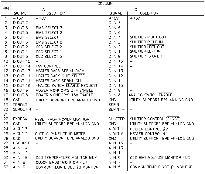
In the above table are the signal assignments for the signals coming from the SDSU Utility board. The columns are organized to show the pins on the 96-pin DIN connector that connects the Utility board to the UCO/Lick Utility Support board. Although the connector has 96 pins, the interconnect cable only passes 64 of these due to the spacing of the ribbon cable. This results in the use of the 'A' and 'C' rows of pins of the DIN-96 connector. On the table, the left-hand column holds the pin number. The rest of the table is divided into two sections, the 'A' pins and 'C' pins.
Pins A1 and C1 pass the -16V and +16v supply voltages of the Utility Support board back to the SDSU Utility board. Pins A18, A26, C16, and C26 are the analog grounds for the power supply voltages. Pins A2 through A17 are the general-purpose digital outputs that the SDSU Utility board provides. We use Dout3 through Dout6 on pins A3 through A6 for select lines that allow us to read back any of the 12 bias voltages that are sent to the CCD dewar electronics box. The bias levels are each brought to an analog multiplexer on the EL-3194 61-pin Cable Interconnect at the back of the chassis. The software can then, via these select lines, read back any of the bias levels that are being sent out to the CCD.
Pins A7, A8, and A9 are the CCD select lines. These are used when multiple CCDs are used in the system and are not applicable to the ESI CCD controller other then they must be set for CCD #0.
Pin A11, Dout14, is wired to the back of the controller on a two-pin connector and is used to turn on and off the cooling fans for the electronics locker that the CCD controller resides in. The two-pin cable runs to a small box labeled 'Fan Control' that contains a solid-state relay that controls the 115V AC to the fans.
Pins A12, A13, and A14, Dout11 through Dout13, are used in systems that require additional heater circuits as in the case of a CCD array. The ESI dewar uses the heater drive that is provided by the SDSU system.
Pin A15, Dout10, is used by the software to turn on the analog switches in the dewar electronics box. This is labeled as a request because the final signal to enable the switches is generated on the EL-1198 Power Monitor board. If the conditions are correct to allow the switches to turn on the Power Monitor board passes this signal. The output that actually goes to the switches also comes back through this connector on pin C17, Din8, so the software will know the actual state of the switches.
A16 and A17, Dout10 and Dout9, are used to tell the Power Monitor board that the software is up and running and it is OK to turn on the +/-16V and +38V supplies to the VME backplane.
Pin A18 is an analog ground.
Pins A19 and A20 are serial I/O lines that we do not use. A21 has no connection.
Pin A22 routes the External Reset line from the Power Monitor board back to the SDSU Utility board. This signal is asserted if the +5V power supply fails,
Pin A23 is a ground
Pin A24 is an analog output that we are currently not using.
Pin A25 is used when a local temperature readout is required on the CCD controller. In the case of ESI, it is not used.
Pin A26 is a ground.
Pin A27 is a current source that is used to drive the temperature diode in the dewar.
Pins A28 and A29, Ain14 and Ain12 are analog inputs that are not used.
Pin A30, Ain10, is an analog input and it used to read back the temperature diode inside the CCD dewar. In multiple CCD applications, different temperature diodes may be read by setting the CCD Select lines to the proper values.
Pin A31, Ain8, is used to monitor the output of any of the clock signals generated in the CCD controller. Each of the SDSU2 Clock Generation boards has the ability to, via software, monitor any of its clock lines and pass it to a SMB coax connector on the front of the board. We route the coaxes to the Utility Support board and apply them to a analog multiplexer. By setting the CCD Select lines to the proper values, clock board outputs can monitored via this pin. Again, in the case of ESI, only one clock board is used and the CCD Select lines are left such that the correct board is always read.
Pin A32, Ain6, is used to read back a second temperature diode if used. In the case of ESI, it is not used.
Pin C1 is used to route the +16V supply voltage to the SDSU Utility board.
Pin C2 through C4, Din5 through Din7, are not used at this time.
Pins C5 through C9, Din0 through Din4, are used to read back the status of the shutter and it's blades. The ESI shutter is made up of two blades that move in and out of the beam. See the EL-1183 write-up in the ESI Spectrograph manual for details.
Pins C10 through C16 are not used.
Pin C17, Din8, is used to monitor the state of the analog switches. This signal is generated on the Power Monitor board.
Pin C18 is a ground
Pins C19 and C20 are serial data inputs. We do not use these lines. C21 has no connection.
Pin C22, SHUTTER, is the shutter control signal. When high, the shutter is open and when low the shutter is closed. This signal is routed out to the EL-3195 Power and Miscellaneous Signal board and then out to the EL-1183 Shutter Controller.
Pin C23 is a ground.
Pins C24 and C25, Aout1 and Aout0, are heater outputs. The SDSU Utility board uses these lines to warm up a heater resistor in the dewar to regulate the temperature. Only Aout0 is used in ESI.
Pin C26 is a ground.
Pins C27 through C29 are analog inputs that are not used at this time.
Pin C30, Ain9, is used to read in the level of the bias voltage that is selected via the Bias Select lines.
Pin C31 is an analog input that is not used at this time.
Pin C32, Ain5, is used to read back the temperature diode that is mounted inside the dewar near the CCD.
Clock Board Signal Assignments, EL-3271
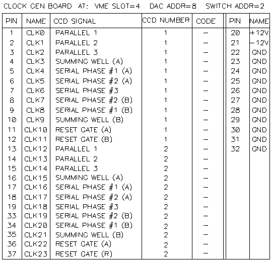
In the above table are the signal assignments for the signals coming from the SDSU2 Clock Generation board. Facing out the front of board is a DB-37 that contains the 24 clock signals, 11 grounds, and connections for the +12 volt and -12 volt supplies on the clock board. We do not connect to the +/-12V lines. Because the CCD only requires 12 clock lines, the 24 clocks are broken up into two sets of 12 each. Column 1 provides the pin number of the DB-37 connector for each signal. The labels in column 2 are the SDSU2 generic clock designations. Column 3 maps the SDSU2 designations into the Lick nomenclature. Column 4 tells which of two possible CCDs that each signal is routed to. The code column is provided for the programming staff. Columns six and seven show the ground and power pins.
For ESI, only the signals designated as CCD 1 in the CCD NUMBER column are used. These include enough signals for either one or two amplifier operation. The parallel clocks as well as SERIAL PHASE#3 are common to both amplifiers, often thought as half of the chip. SUMMING WELL(A), SERIAL PHASE#1(A), SERIAL PHASE#2(A), and RESET GATE(A) are unique to each half of the device.
Video Board Signal Assignments, EL-3282
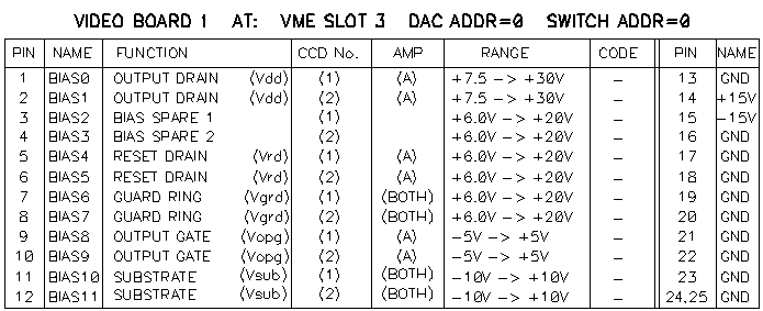
In the above table are the signal assignments for the signals coming from the SDSU Video Processor board. Facing out the front of board is a DB-25 that contains the 12 bias levels, 11 grounds, and connections for the +15 volt and -15 volt supplies on the video board. We do not connect to the +/-15V lines. Because the CCD only requires 5 bias levels, the 12 bias levels are broken up into two sets of 6 each. This provides a OUTPUT DRAIN, RESET DRAIN, GUARD RING, OUTPUT GATE, SUBSTRATE, and a spare bias level connection for each of two possible CCDs.
Column one provides the pin number of the DB-25 connector for each signal. The labels in column two are the SDSU2 generic bias level designations. Column three maps the SDSU2 designations into the Lick nomenclature. Column four tells which of two possible CCDs that each signal is routed to. Column five maps out which amplifier in a two-amplifier system that each signal would be applied to. Columns six shows the range of the individual bias levels. The code column is provided for the programming staff. Columns seven and eight show the ground and power pins.
For ESI, only the signals designated as CCD 1 in the CCD NUMBER column are used. These include enough signals for either one or two amplifier operation. The OUTPUT DRAIN, RESET DRAIN, and OUTPUT GATE are common to both amplifiers, often thought as half of the chip. SUMMING WELL(A), SERIAL PHASE#1(A), SERIAL PHASE#2(A), and RESET GATE(A) are unique to each half of the device.
61-pin Cable Signal Assignments, EL-3172
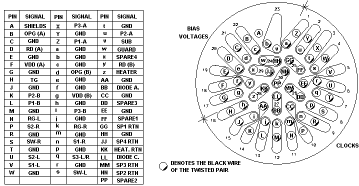
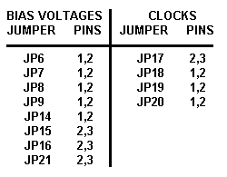
In the above table are the signal assignments for the signals that leave the CCD controller on the large umbilical cable. As many of these signals are generic, to determine which are in use for any particular application please refer to the jumper setting tables on sheet 5 of the EL-3194 schematic.
In the case of ESI, the jumpers are set as shown above and in the entry for the MITLL single amplifier application. The results of the jumper placement are as follows:
BIAS0 from the SDSU2 video board, OUTPUT DRAIN(A) is sent out on pin 'F' of the 61-pin connector via JP14
BIAS0 is also sent out on pin 'g' via JP15
BIAS4, RESET DRAIN is sent to pin 'D' via JP9
BIAS4 is also sent out on pin 'y' via JP16
BIAS8, OUTPUT GATE(A) is sent out on pin 'B' via jumper JP7
BIAS8 is also sent out on pin 'd' via JP21
BIAS10, SUBSTRATE is sent out on pin 'v' via JP6
BIAS6, GUARD RING is sent out on pin 'w' via jumper JP8
The TRANSFER GATE line is not used and it's wire is tied to ground via JP17
CLK0, PARALLEL1 is sent out on pin 'L' via jumper JP20
CLK1, PARALLEL2 is sent out on pin 'K' via jumper JP19
CLK2, PARALLEL3 is sent out on pin 'i' via jumper JP18
The other bias levels and clocks are 'hard wired' and stay with their associated pins as shown on the first diagram. The cable also has an overall shield braid. The shield is soldered to lengths of wire that exit from the back of the connectors and connect to the chassis' at both ends via banana plugs.
17-pin Cable Signal Assignments, EL-3173
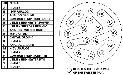
In the above table are the signal assignments for the signals that leave the CCD controller on the 17-pin power cable. All of the named signals are used in all CCD controllers. At this time however, none of the spare lines are in use and are reserved for future use. The drawing above also shows how the wires are grouped into twisted pairs. The cable also has an overall shield braid. The shield is soldered to lengths of wire that exit from the back of the connectors and connect to the chassis' at both ends via banana plugs.
![]()
![]()