ESI CCD Electronics Manual
![]()
![]()
![]()
Board Designs:
The Eshelette Spectrograph and Imager, ESI, instrument has been built by the Technical Facilities department of the University of California Observatories, Lick Observatory, UCO/Lick Observatory. This manual will cover the CCD Controller. The Instrument Controller is covered separately in the ESI Instrument Manual.
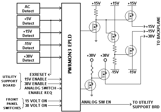
The Power Monitor card is used in most of the UCO/Lick Observatory CCD Controllers. It monitors the voltage levels of the power supplies, the AC voltage level and accepts inputs from the SDSU Utility board and front panel switches. Using these inputs an Altera programmable logic chip determines if the +16V, -16V, and +38V supplies may be supplied to the VME style backplane and in what order. The idea is to allow the +/-16V to be supplied to the backplane only if all of the voltages are above a predetermined level, the Utility board program is ready for them, and the front panel switch is set to on. The 38V to the backplane will only be supplied if the above conditions are true and the 16V supplies are already enabled. The Altera chip incorporated a delay between when the 16V is enabled and the 38V is enabled.
The 16V and 38V supplies are used to supply the DACs on the SDSU Analog board that supply bias voltages and clock waveforms to the CCD. Because of this we want the 16V and 38V supplies held off until the programming can setup the DACs and thus keep spurious voltages off of the CCD chip. As the block diagram indicates, the Altera chip provides the logic functions for the board. It contains the coding 'monpwr3'. It should be noted that the voltage sensors that are used only sense voltages lower than a set point and do not give an indication of an over voltage condition.
Detailed description:
120V AC is applied to pins 1 and 7 of the input connector J1 and from there to pins 1 and 4 of the HCPL3700 optocoupler through R1-R2 and R3-R4. These resistors set the turn on point of the optocoupler to be about 108V AC. Thus if the line voltage falls below this point the normally low output of the chip will go high signaling a failure of the AC line. U2, a TL7705A Supply Voltage Supervisor, has its sense input tied to the 5 volt supply via a 100 ohm resistor. In this configuration the output will become active (low) if the input drops below 4.55-4.6 volts. Its output is also sent back to the Utility board as the EXRESET, external reset, signal to the SDSU system. U3 is a TL7715A which is a 15 volt version of the TL77xx. It's threshold is set to 13.8 volts by internal resistors. U4 is another TL7715A but it has it's ground input set to -16V and it's sense input tied to ground so that it can sense the negative voltage. The threshold is now -13.8 volts. The generic version, TL7702A, is used to sense the +38V supply by using a voltage divider at the input. If the voltage at the sense input goes below 2.5 volts the output will become active.
Besides the inputs from the voltage sensors, the circuit accepts logic inputs from the Utility board. These come in on J2 and are comprised of '15V ENABLE', '38V ENABLE', and 'ANALOG_SW_EN_REQ'. These are all fed directly into the Altera chip on pins 10, 60, and 13 respectively. Also, the RESET output of the 5V-supervisor chip is fed back to the Utility board as EXRESET, the external reset. Note: for test purposes, a test connector with pins 5, 6, 7, & 8 shorted can be connected to J2 to eliminate the need for having a working Utility board during testing. The board also receives inputs from the front panel enable switches MAN 15V ON and MAN 38V ON via J3. These switches are used for local control of the voltages to the controller backplane. Logic in the EPLD ensures that the front panel switches can only turn on the power supplies if the software has already enabled them. Thus, both the software and the front panel switches must be set to get the power applied to the backplane. Also, a shorting block, W1, is provided for backwards compatibility with older controllers that don't use the control bit for enabling the analog switches in the CCD electronics box.
G7, an LM555 timer, provides a 100KHz clock to the clock input of the Altera chip. The EPLD uses this as a time base to determine the various delays within the chip. These are seen as the delay between the turn on of the 16V supplies and the 38V supply and the delay needed for recovery of the 16V supply from the current inrush when the MOSFET turns on. The Altera chip 'monpwr3' provides the logic to determine the states of its three output pins. The outputs are 15ON, 38ON, and ANA_SW_ENABLE. The 15V ON signal turns on MOSFET Q2 which in turn turns on Q4 which passes the +15 volt supply to pin 6 of J6 and on to the backplane. In a similar manner, when Q2 turns on, Q7 also turns on. This causes MOSFET Q6 to turn on and pass the -16V supply to pin 8 of J6. The 38ON signal and MOSFETs Q3 and Q5 work in a similar fashion. The last output of the EPLD is the ANALOG_SW_EN. The logic of the EPLD only allows this output to go high if both the ON15 and ON38 are enabled.
EPLD description:
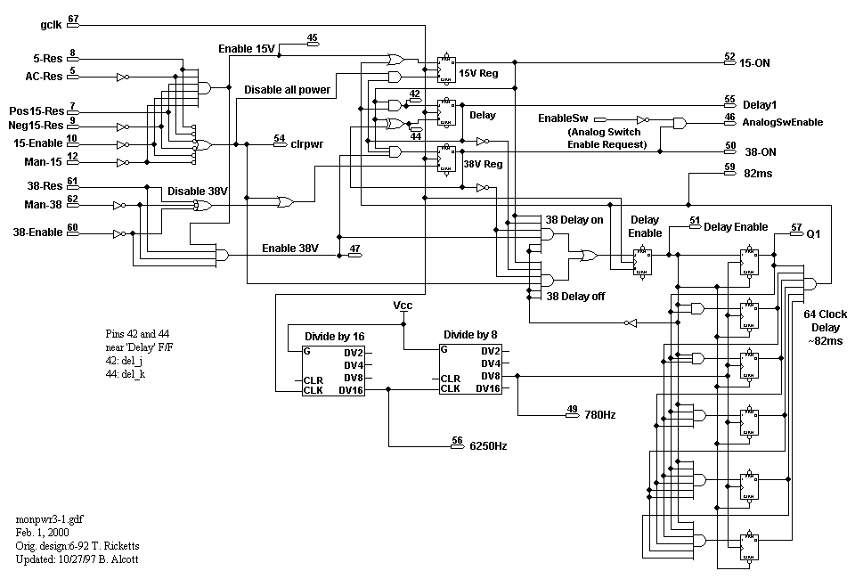
Power Monitor EPLD - monpwr3
The Altera EPLD used on this board is an EPM7064LC68. This device has 64 macrocells, 48 I/O pins, and 1,200 usable gates. The chip can be programmed with the proper hardware and easily erased with a UV source. We have used both hardware and software from Altera. The schematic, timing diagram, and project report has been provided with the Power Monitor schematic.
At the top of the drawing is the input for the 100KHz on pin 67. This clock provides all of the timing functions. At the top center of the diagram are three JK flip-flops. Two of these are the output control registers for the power supply enables. Output pin 52 (top flip-flop) will, if high, enable the +/- 16V supplies. Pin 50 (bottom flip-flop) will, if high, enable the 38V supply. The center flip-flop allows the delay counter to start. The purpose of the delay is to control the sequence of that application of power. We want the +/-16V supply to come on before the +38V supply. This will insure that the DACs on the SDSU clock board will have power before the voltage that they control is present. This will prevent dangerous, uncontrolled voltages from being applied to the CCD. When the power is being shut down we also want to sequence the power supplies such that the +38V is removed before the +/-16V is removed. An 'and' gate at the output of the 38-ON is used to ensure that the analog switches in the dewar electronics box will not come on unless the voltages to the DACs is applied properly.
The six input 'and' gate at the top left of the diagram controls the enabling of the +/-16 volts. It will be enabled if the +5V, +/-16V, and AC line are within the proper range; the signal from the front panel toggle switch is present, and the enable from the SDSU Utility board is present. If these conditions are met the '15-ON' flip-flop will be set, and will enable the +/-16V to be applied to the backplane.
The output of the 'and' gate is also routed to a 4 input 'and' gate at the bottom of the left-hand edge of the diagram. This gate will be enabled if all of the conditions for the +/-16V, the +38V supply is in proper range, and the enable signal from the front panel switch is present, and the Utility board enable is present. At this point a sequence of events will occur. A 3 input 'and' gate leading to the 'J' input of the ON-38 flip-flop will have two of its inputs enabled. The third input comes from the 'delay' flip-flop that will not yet be set. In the center of the sheet are two 6 input 'and' gates. The top one, labeled '38 Delay on' will now be enabled. The next clock cycle will set the 'Delay Enable' flip-flop. This will, via the inverter, disable the input so it will not continue to be set and will enable the six bit counter. When all six bits of the counter are high the 'Delay Enable' flip-flop will be reset and the 'Delay' flip-flop will be set. This will happen after 64 clock cycles or about 82 milliseconds. The two frequency dividers in the center of the page have been added to lengthen the delay time from the original 0.7 milliseconds to approximately 82 milliseconds. This provides ample time to allow for the momentary spike on the +16V supply due to the current in rush at turn on. When the 'Delay' flip-flop is set the '38-ON' flip-flop will be enabled and will clock high on the next clock. The output of the '38-ON' flip-flop will cause the 'Delay' flip-flop to be reset on the next clock.
All of the of the inputs to the input to the 'Enable-15' 'and' gate are also sent to a six input 'nor' gate. If any of these signals are absent the gate will produce the 'clrpwr' signal on pin 5. This signal is routed to a two-input 'or' gate. The other input to the 'or' gate comes from a three input 'nor' gate tied to the three enable lines for the +38V. If any of these enable signals are not present the two input 'or' gate will cause the '38-ON' flip-flop to be reset. Then the six input 'and' gate labeled '38 Delay off' will be enabled causing the delay cycle to start. At the end of the 64 clock cycles the 'Delay' flip-flop will be set. This will cause the '15-ON' flip-flop to be reset on the next clock if the delay was caused by the 'clrpwr' signal. A loss of the 38V alone will not reset the flip-flop. The 'Delay' flip-flop will be cleared when the other two flip-flops are either both set or both reset.
Dual Pre-Amplifier Board, EL-1220
This board resides in the electronic box and takes its inputs from the hermetic SMA connectors mounted on the dewar wall. The SMA connectors are passing the ac-coupled CCD video output signal from the MITLL CCD Interconnect Board, EL-1240.
The Dual CCD preamplifier board consists of 2 independent CCD preamplifiers whose discrete component values can be individually changed if neccessary to match the needs for a given CCD.
Each CCD preamplifier is a low noise, wide bandwidth non-inverting operational amplifier that can drive 50 ohm coax cable for a distance of 10 feet or more without any sacrafice in speed. Looking at preamplifier A on sheet 2, the gain of the preamplifier is set by resistors R19 and R22: Gain = 1+R19/R22. For ESI's MIT/LL CCD the gain of each preamplifier is set at 5.5. The matched JFET pair J1 is the preamplifier's differential input. The differential signals work their way to U1, the AD829 op amp. Resistors R11 and R17 set the gain of the differential signals to the AD829. The AD829 provides the differential to single-ended open loop gain and passes its output to an output buffer, composed of transistors Q1, Q2, Q6, Q7. Capacitor C17 sets the overall bandwidth of the preamplifier and is needed for stability. Capacitor C26 is also required for stability to slow the AD829's response since the AD829 is being used in an open loop configuration. Diodes D1 and D2 prevent the preamplifier from becoming saturated when the CCD's reset gate pulse occurs by clamping the output of U1 to 6.6 volts. The clamp has no effect on the CCD video output which is a negative going pulse.
The output from each preamplifier is passed through SMA connectors to the electronoc box's BNC video connectors. From there each CCD preamplifier video output signal is sent via 50 ohm coax approximately 10 ft. to the SDSU-2 CCD Controller's back panel. The video signals are then passed to the SDSU-2 video board to be digitized.
Dewar/Hermetic Connector Board, EL-1227
This board lives inside the dewar. It is soldered directly to the back of the 61-pin hermetic connector. It breaks the signals up into two sets which each then go to a 32-pin Ohmnetics connector. This board is used in all of our recent dewars.
MITLL CCD Interconnect Board, EL-1240
This board lives inside the dewar. It is laid out specifically for the MIT/Lincoln Labs CCD as used in the ESI dewar. This board does the 'cross wiring' that matches the generic incoming signals from the EL-1227 board to the connector from the CCD. It also has the AC coupling capacitors for the video output from the CCD. Lastly, it provides a 4-pin connector for the temperature diode and the heater resistor.
17-pin Connector/Power Filter board, EL-3191
This board lives at the dewar inside the electronics box. It is designed to filter the DC power coming from the CCD controller chassis and to pass the heater, temperature, and analog switch signals. It consists of input and output connectors, PI filters on the 5, +16, and –16 volt power lines, and an Opto-isolator for the analog switch enable signal. Sheet 1 shows the inputs to the board on connector P1. To the right of the connectors is shown the filtering on the DC voltage lines. The filtering consists of the 820 mH inductors and the 100 m F capacitors. The 1.0 mF and 0.1 m caps provide a low impedance path to ground for any AC noise.
On the upper left-hand side of sheet 2, P2 connects the heater resistor and temperature diode signals as follows:
P1 pin D to P2 pin 1 – COM_TEMP_DIODE The temperature diode in the dewar.
P1 pin P to P2 pin 2 – COM_TEMP_DIODE_RTN
P1 pin E to P2 pin 3 – UTIL_HEATER The heater resistor in the dewar.
P1 pin R to P2 pin 4 – UTIL_HEATERBelow P2 is the circuit that isolates and buffers the analog switch signal. The ANALOG_SW_EN-IN signal comes in on pin G of P1. Also, a connection to the utility support board’s 5-volt supply comes in on pin F of P1. These two inputs connect to the 4N35 opto-isolator at U1. When the ANALOG_SW_EN-IN signal is driven low, the output of the isolator also goes low. This level is applied to the input of the 74LS240 bus driver chip and as the output is inverted, output 1 is then routed to the other drivers of the chip. The final outputs are then the same sense as the input signal. These outputs are then routed to the Analog Switch Board connectors P5, P6, P7, and P8 (shown on the right-hand side of the page.) At the bottom left-hand side of the page is a set of spare contacts for future use or customization.
The middle column of connectors are for the CCD pre-amplifiers in the dewar electronics boxes. Pin 1 connects to the output of the +16V onboard filter, pin 3 connects to the –16v filter and pins 2 and 4 provide analog grounds to the pre-amps. The right-hand side column of connectors provide connections for the Analog Switch boards. These connectors provide the following connections:
Pin 1 +5 volt logic supply
Pin 2 5 volt ground (digital ground)
Pin 3 ANALOG_SW_EN_n
Pin 4 no connection
Pin 5 +16 volt analog supply
Pin 6 +16 volt ground (analog)
Pin 7 -16 volt analog supply
Pin 8 -16 volt ground (analog)Note: this board was designed to provide interconnections for from 1 to 4 CCD signal chains. In DEIMOS, three of these boards are used. Two of which connect four channels each and a third that connects only two channels. In ESI, there is only a single board used as there is only one CCD used.
61-Pin Connector/Analog Switch Board, EL-3192
This board lives in the dewar electronics box and was designed to receive the umbilical cable from the CCD controller and provide isolation of the bias voltages from the CCD chip in the dewar. The board contains six DG411 quad analog switches, two transistors, two optical isolators, and various filter and bypass capacitors.
Sheet 1
The first page of the schematic shows that 61-pin connector P1 that receives the umbilical cable from the CCD controller on the left-hand side. On the right-hand side is the power input connector P2. The power is divided into two sections, the 5 volt logic (digital) supply and the +/- 16 analog supplies. These supplies are isolated from each other to lessen noise on the bias voltages. Also shown is the ANALOG_SW_EN signal arriving on pin 3 of P2. R1 is used as a pull-up for the ANALOG_SW_EN signal. Along the bottom of the sheet is the filtering and bypassing component for the +/- 16 volt supplies.
Sheet 2
This sheet has two columns of analog switches. In each case, a clock signal is presented to the input of a switch and the resulting signal has OUT appended to its name. All of the clocks are pulled down to ground so that if a cable is disconnected or a wire breaks the output of that particular switch won’t have a potentially harmful voltage on it’s output that is connected directly to the CCD chip. As is shown on the schematic, each of the clock lines also has a small filtering/bypass capacitor on it’s output. These switches are all enabled by the ANALOG_SW_EN signal. This enable signal allows the computer to set the clock waveforms as needed before they are allowed to go to the CCD chip. This way we can insure that no incorrect levels are applied to the chip during that time it takes to load the waveforms.
Sheet 3
This sheet shows the bias voltages that go to the CCD chip. On the right-hand side are the RD (reset Drain) and OPG (output gate) levels. There are two each of these signals used for a two-amplifier CCD chip. Note that these signals are held at DC levels and therefor have more filtering on the outputs. On the left-hand side of the sheet are the VDD, SUB, and Guard signals. The SUB (substrate) and Guard (guard ring) levels are again presented to an analog switch using the ANALOG_SW_EN signal to enable the outputs. On the other hand, the VDD levels are potentially beyond the allowed voltage for the analog switch so we use a different set of components to enable and disable these levels. An optical isolator is used to drive the MOSFET switch which when turned on passes the VDD level.
Sheet 4
The top of this sheet shows the spare circuits that are on the board. Note that in the case of spare 1 and spare 2, that a jumpers JP4 and JP6 are provide at the analog switch’s input. These should be installed into the grounded position to keep the spare 1 and spare 2 signals that come through umbilical cable free of noise. Again, the other non-switched spares and returns should similarly jumpered to ground. At the bottom of the sheet, are output connectors P3 and P4. These connectors contain all of the signals and levels that go directly to the CCD plus that lines for the temperature diode and heater resister. P4 to the left contains the clock signals and P3 contains the bias levels. The mates to these connectors are hand-wired twisted pairs with grounds on one side of the connector and the signal on the other side. These are wired to the 61-pin connector that mates with the hermetic connector in the dewar.
Utility Support Board, EL-3193
(Also see EL-3162.) This board lives in the CCD controller chassis and was designed to break out the various signals that originate on the SDSU utility board. In essence, we are using the general digital and analog I/O bits to accomplish the various auxiliary functions needed for the operation of the CCD controller.
Sheet 1
The top of this sheet shows the 96-pin din connector that is wired pin-for-pin to the Utility Support board. The signals that are used are all labeled. Notice that the connector on the right side of each group, P1, is used as a test probe connector for troubleshooting. This connector faces directly out from the board and the interconnecting cable from the Utility Support board is attached to the connector behind it. On the bottom of the sheet is, on the left-hand side, P7 that brings in the power for the board. As with the other cards in the system, the +5 volt logic ground is separate from the +/- 16 volt analog ground. The middle, bottom of the drawing is the local filtering for the power supply voltages. On the bottom right-hand side of the sheet is a connector, P8, that can be used in applications where a local readout of the temperature of the dewar is required. This, of course, requires specific programming to be in place to be implemented.
Sheet 2
(Also see EL-1187) This sheet shows the connections for the Power Monitor board. The Power Monitor board monitors the voltages of the various power supplies and sends signals to the SDSU2 system if any of the supplies fail. It also enforces the sequence in which power can be applied to the dewar electronics. It will not let the ANALOG_SW_EN signal to be asserted unless the +38 volt supply in on and up to voltage. In turn, it will not allow the +38 volt supply to turn on until the 16 volt supplies are on and up to voltage. The 16 volt supplies will not be allowed to turn on unless both the 5 volt supply is up and the 120 VAC is within limits. Beyond this, the Utility Board, under program control, must also send enables to the power monitor board. These signals are shown on the left-hand side of this sheet. Each of them are feed through opto-isolators to buffer them and protect that CCD controller in case of over voltage, line spikes or other failures. The signal ANALOG_SW_EN_REQ is sent by the controller as a request to the Power Monitor board. If the conditions are right and the Power Monitor does enable the switches, that enable signal comes back on pin 5 of P9 where transistor Q20 and optic isolator U11 convert the signal and apply it to the 74LS240 line driver. After an inversion of the signal, it is routed to both the analog switch boards via P14 (sheet 3) and back to the Utility Support board via pin C17 of connector P2 (sheet 1.) The EXRESET signal is sent from the Power Monitor if the 5 volt supply goes below its set point of about 4.6 volts. Again, the signals on the left side of the sheet, ANALOG_SW_EN_REQ, 15V_ENABLE, and 34V_ENABLE are outputs sent to the Power Monitor and the signals on the right-hand side are signals returning from it.
Sheet 3
This sheet is concerned with the signals that enter and exit on P14, and go to the EL-3195 Power and Miscellaneous Signal board. The opto-isolators at the top of the page are used to input signals that originate at the Shutter Controller Box, EL-1183. These signals are read back on digital input bit Din0 through Din4 and inform the controller of the status of the dewar shutter. Also at the top is the shutter output signal SHUTTER_CLOSE. This signal is high when the controller wants the shutter open and low when it wants it closed. This signal is also isolated to protect the CCD controller. At the lower left-hand side of the drawing are the heater and temperature diode lines. The temperature diodes are connected to a constant current source shown on sheet 4. The voltage developed across the diode arrives at the board on pins 15 and 24 of P14 and is then fed to analog inputs on the Utility board via pins A32 and C32 of the connector P2 (sheet 1.) The heater voltages originate on the SDSU Utility board as analog outputs Aout1 and Aout2. These signals go directly to the resistor(s) mounted in the dewar via pins 17 and 22 of P14 (and then through the Power and Miscellaneous Signal board.) The controller monitors the temperature of the CCD and regulates it via these heater resistors.
Sheet 4
This sheet shows the available extra temperature diodes that can be mounted in the CCD dewar. For mosaics like the DEIMOS project, these can be used to monitor the temperatures at the various CCDs. The normal configuration of a single CCD chip works fine with the two temperature diodes available with the normal SDSU system but with a mosaic of chips two temperature inputs are generally not enough to give a good picture of what is going on in the dewar. Thus the Utility Support board supplements the system with an additional temperature diode circuit for each of the controller’s signal chains. To do this, the constant current drive circuit is replicated eight times with a unique drive available at each of the CCD connectors P3 through P6 and P10 through P13. In the lower right-hand portion of the sheet is an analog multiplexer. Each of the above mentioned current drive circuits are also wired to an input to the multiplexer. The controller can read any one of these eight levels by selecting the CCD of interest on the CCD select lines CCD_SEL_0 through CCD_SEL_2 and reading the corresponding level on the Utility board’s analog input Ain10. Op-amp U26 buffers the output of the multiplexer before it is sent to the Utility board.
Sheet 5 and Sheet 6
These sheets are identical except for the circuit number. Sheet 5 contains heater circuits for CCDs 1 through 4 and sheet 6 contains heater circuits for CCDs 5 through 8. At the bottom left of sheet 5 is a precision 10 volt reference circuit for the serial DACs U12 and U13. The LT1021BCN8-10 is a precision 10 volt reference IC. The LT1097CN8 is a low noise op-amp that employed to regulate the output of the circuit via the feedback resistor R95. The MAX536BCPE is a quad, 12-bit D/A with a serial input. The control signals for the DACs consist of a serial clock, DACS_SCLK, the serial data, DACS_SD1, and the chip select DACS_CS. The serial data is daisy chained from U12 to U13. In brief, these chips accept serial data when the CS signal is pulled low and act on it when the CS goes back high. The serial data is transferred in 16-bit words with the four MSB bits containing address and command information. The other 12 bits contain the D/A value to be output by the selected DAC. (http://dbserv.maxim-ic.com/quick_view2.cfm?pdf_num=1125) Each of the four analog outputs are wired to a voltage follower/current source. These supply the power to drive four, or between both sheets, eight extra heater resistors that can be mounted on the mosaic backplane. The outputs of these circuits go to pin 2 of the CCD connectors P3 through P6 and P10 through P13.
Sheet 7
(Also see EL-3161) The eight connectors at the top of this page distribute the heater drive, temperature readout, and power supply voltages to the EL-3194 CCD cable interconnect boards. Also, each connector has a BIAS_MUX_CCDn signal that returns from the cable interface board. This is explained in the EL-3194 write-up but in essence, we are able to read back any of the bias levels that are sent out to the CCD dewar on this line. Each of these lines is wired to the analog mux at U18 in the lower left-hand area of the diagram. The CCD_SEL lines can then be set to read any one of these bias levels back via the buffer amplifier U27 at analog input Ain9 of the SDSU Utility board.
Sheet 8
(Also see EL-3161) The last sheet shows the connections from the Clock Interconnect boards. Each of the SDSU2 Clock Driver boards is capable of sending a waveform out on an SMB connector at the front of the board. This allows us to monitor any one of the clock waveforms by the following procedure: first, select its address internally on the clock board, next, set the CCD_SEL address via the Utility board, and finally, read the CLOCK_MUX_OUT signal at analog input Ain8. For single or dual chain controllers only the signal from Clock Board #1 is available. In other configurations, as many as five Clock Driver boards may be in the system.
61-pin Cable Interconnect Board, EL-3194
(Also see EL-3161.) This board lives inside the CCD controller and its primarily function is to gather all of the signals generated within the CCD controller for a single CCD and connect them to the umbilical cable which delivers them to the CCD dewar electronics box. One nice feature of this board is that it has an external connector, P3, with each of the board’s signals available for troubleshooting the system.
Sheet 1
In the upper left-hand of the drawing is connector P7. This cable brings in the heater, temperature diode, and bias select signals and sends out the selected bias voltage via pin 12. This is also where the +5 volt and +/-16 volt supplies enter the card. Below P7 is the onboard filtering of the supply voltages. Again, notice that the +5 volt ground is kept separate from the +/-16 volt analog ground. The right side of the drawing shows the 61-pin MS-style connector that connects the CCD controller to the dewar. An attempt has been made here to pass as many ground signals as possible through the cable. What doesn’t show up here is the overall shield connection for the cable. This is done using a banana plug and jack arrangement where length of wire is soldered to the shield and is terminated into a banana plug which is then connected to a jack on the back of the chassis.
Sheet 2
This sheet shows the connectors that bring the clocks and bias voltages from the SDSU2 clock and bias boards. The connector P4 receives the bias voltages for the first CCD amplifier that is used in the chain. If a second amplifier is available on the CCD, it’s signals come into the board via P6. P2 receives the clock signals from the clock driver board. P5, if used, brings in the extra clock signals for frame transfer devices or for the transfer gate of a Lick/Orbit CCD. The rest of the sheet shows the various jumper options available on the board. These are determined by the configuration of the CCD chip used in the dewar. Also, see sheet 5 as a guide for configuring these jumpers.
Sheet 3
This sheet shows the various circuits used to read back the bias levels that are being sent to the CCD chip. The upper left hand circuit show the bias level RD(A). Due to the input range of the ADC (sheet 4), this level is divided by ten via the precision resistor network RN4. This level is then wired into the op-amp U1 voltage divider. The resistor network RN3 in the feedback loop presents the same impedance as is seen at the non-inverting input and compensates for any bias current flowing into that input. The other circuits work in the same manner. Notice however, several of the circuits do a division by two rather than ten. This is due to the normal level expected on these bias levels. Notice too that the signals that actually go out to the CCD are the levels that show up as inputs on this page. The outputs of these circuits are fed only to the analog multiplexer and then back to the CCD controller for monitoring purposes only.
Sheet 4
This sheet contains the analog multiplexer that selects the bias level to be read back into the CCD controller. Under software control, the four select lines can be set to read in any of the eight biases or four spare levels on the board. In practice, none of the spare lines have yet to be used in any of the controllers. The output of the multiplexer is wired to a voltage follower circuit that sends it’s output to pin 12 of P7 and back to the Utility board via the Utility Support board. Below the multiplexer is a set of jumpers. Each of these jumpers can be inserted to tie its signal line to ground. Again, these lines are not presently used and the jumpers are normally installed to keep the wires in the umbilical cable from floating. On the right-hand side of the page is the test connector that sticks out of the panel on which the board mounts and provides scope probe access to any of the signals on the board. This of course is meant as a troubleshooting aide and does not have a mating connector.
Sheet 5
The final sheet gives the jumper settings for the various configurations of the CCDs that the controller supports at this time. It is hoped that the controller has been made general purpose enough that future CCDs will be able to be accommodated with only jumper and cabling changes.
Power and Miscellaneous Signal Interconnect Board, EL-3195
(Also see EL-3161.) This board lives inside the CCD controller. The boards major function is to receive signals and power supply voltages and then send them out to the CCD dewar electronics box. The board is set-up to supply two CCD signal chains. That is, it contains two sets of input and output connectors for power and miscellaneous signals. It also has an output connector for communicating with the EL-1183 Shutter Control box. This board can be loaded for either one or two CCD signal chains. If only one CCD is to be used, the connectors P4 and P6 are not installed.
Sheet 1
At the top left-hand corner of the drawing are two connectors, P1 and P4. These connectors are wired directly to the indicated power supplies. Below these connectors is P5, which sends and receives signals from the Utility support board. The output signals consist of temperature control lines, the shutter command signal, and the analog switch enable. The +5VD-UTIL_SUPPORT_1 line is the 5 volt line that originates on the EL-3193Utility Support board. This line is passed along to the EL-3192 analog switch board to allow the use of an opto-isolator to receive the ANALOG_SW_EN signal. With the exception of the SHUTTER_CLOSE signal, all of the other shutter related signals are status line that go back to digital inputs on the SDSU Utility board. On the right-hand side of the sheet is the DB9 connector that connects to the EL-1183 Shutter Controller. Again, the SHUTTER_CLOSE signal is an output and the rest of the signals are input from the shutter controller.
Sheet 2
The top half of the sheet shows the two 17-pin MS-style output connectors. These connectors are mounted on the panel that screws onto the back of the CCD controller chassis. The cable from this connector, along with the umbilical cable, are the two cables that connect the CCD Controller with the CCD dewar electronics box(es). Each connector passes the +5 volt and +/-16 volt power supply voltages. Also passed are the heater, temperature diode, and analog switch enable signals. The bottom of the sheet shows the spare signal lines that are available for future use. When not in use, these jumpers should be installed to tie the associated wires in the cable to ground.
CLOCK CABLE INTERCONNECT TYPE-1, EL-3198
This board lives in the CCD controller and is designed to take the clock signals from two San Diego State University 2nd Generation Clock Boards and divide them up between four CCDs. There are no components on the board other then the connectors so there is no maintenance or testing needed on a board that has been installed into a system. Also see EL-3164 sheets 1 and 2 for more details.
BIAS CABLE INTERCONNECT, EL-3199
This board lives in the CCD controller and is designed to take the bias voltages from two San Diego State University 2nd Generation Video Boards and divide them up between four CCDs. There are no components on the board other then the connectors so there is no maintenance or testing needed on a board that has been installed into a system. Also see EL-3163 sheets 1, 2 and 3 for more details.
![]()
![]()
![]()